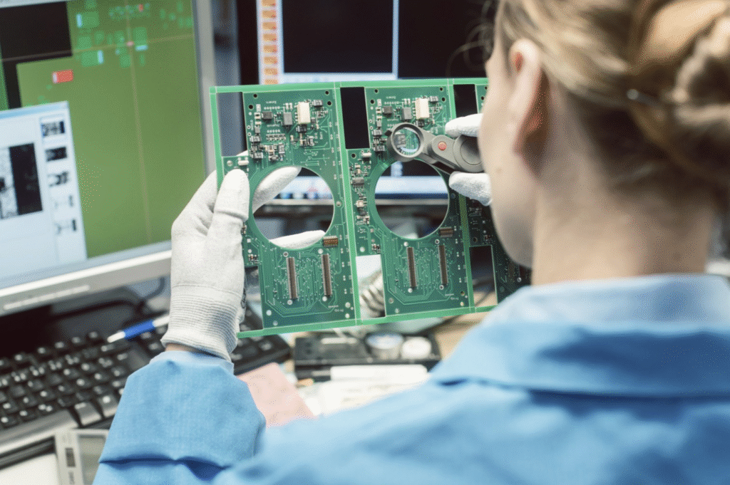
Introduction
PCB short circuit is sues are among the most critical reliability risks in modern electronics manufacturing. In modern electronics manufacturing, PCB reliability is no longer just a quality metric—it is a business-critical factor that directly impacts product performance, brand reputation, and long-term customer trust.
Among all PCB defects, short circuits remain one of the most destructive and complex failure modes. Unlike open circuits, which typically result in immediate and detectable functional failure, short circuits can behave unpredictably. Some appear instantly during testing, while others remain latent—only emerging under electrical load, environmental stress, or prolonged operation.
This delayed failure characteristic makes short circuits particularly dangerous in high-reliability applications such as industrial control systems, automotive electronics, and medical devices.
More importantly, short circuits are rarely caused by isolated mistakes. In most cases, they are the result of accumulated process deviations across:
- PCB design
- Fabrication
- Assembly
- Environmental control
This article provides a deep technical breakdown of PCB short circuits, covering not only what causes them—but how they develop, how to detect them effectively, and how to eliminate them through process-level control.
What Is a PCB Short Circuit?
A PCB short circuit occurs when two conductive elements that are intended to remain electrically isolated become unintentionally connected, forming a low-resistance path.
Electrical Perspective
From an electrical standpoint, a short circuit leads to:
- Current exceeding design limits
- Voltage drops across unintended paths
- Localized heat generation
In severe cases, this can result in:
- Component burnout
- Trace damage
- Power supply failure
To better understand how PCB short circuit defects are introduced during production, it is important to review the full PCB assembly workflow, especially soldering and inspection stages. For a detailed breakdown, see PCB assembly process step by step.
For a general electrical explanation of short circuits, see PCB short circuit definition.
Types of PCB Short Circuits
| Type | Description | Detection Difficulty | Typical Scenario |
|---|---|---|---|
| Hard short | Direct metallic connection | Easy | Solder bridge |
| Soft short | Partial/unstable connection | Medium | Contamination |
| Intermittent short | Appears under conditions | Hard | ECM or thermal stress |
| Latent short | Develops over time | Very Hard | Ionic residue + humidity |
Understanding these categories is critical because not all short circuits behave the same—and not all can be detected at the same stage.
Root Causes of PCB Short Circuits (Deep Dive)
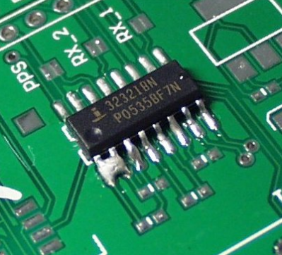
1. Solder Bridging in SMT Assembly
Solder bridging is statistically the most frequent cause of PCB short circuits in high-density assemblies.
Process-Level Root Causes
| Process Step | Failure Mode | Explanation |
|---|---|---|
| Solder paste printing | Excess volume | Too much paste leads to overflow during reflow |
| Stencil design | Improper aperture | Aperture too large or poorly shaped |
| Placement | Misalignment | Offset components cause solder merging |
| Reflow | Overheating | Excessive wetting spreads solder |
Engineering Insight
Fine-pitch components (<0.4 mm) dramatically increase bridging risk due to:
- Reduced pad spacing
- Capillary solder flow behavior
- Surface tension effects during reflow
Even minor deviations in stencil thickness (±10 µm) can significantly impact bridging probability.
2. PCB Fabrication-Induced Shorts
Many engineers underestimate how often short circuits originate during PCB fabrication.
Critical Fabrication Risks
| Area | Risk Mechanism | Why It Happens |
|---|---|---|
| Etching | Copper residue | Incomplete etching process |
| Inner layers | Misregistration | Layer alignment error |
| Via holes | Conductive debris | Poor desmear/cleaning |
| Plating | Overgrowth | Excess copper deposition |
Key Challenge
Fabrication defects are often:
- Invisible after lamination
- Undetectable by AOI
- Only found during electrical testing—or worse, in the field
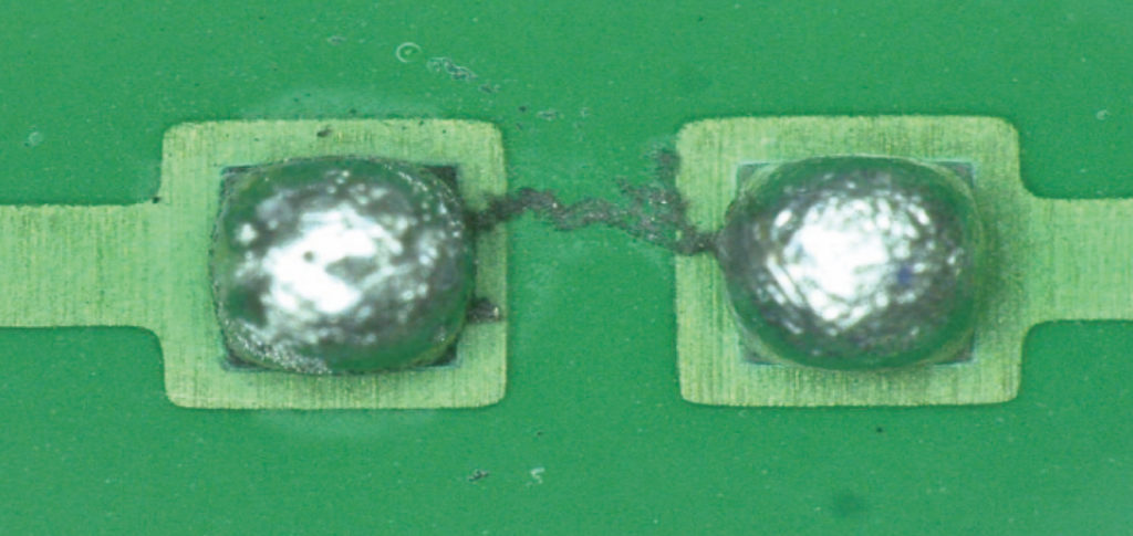
3. Contamination and Electrochemical Effects
This is one of the most underestimated causes of latent short circuits.
Types of Contaminants
- Ionic residues (flux activators, salts)
- Organic residues (flux, oils)
- Environmental particles (dust, fibers)
Electrochemical Migration (ECM)
Under bias voltage and humidity:
- Metal ions dissolve and migrate
- Conductive dendrites grow between conductors
This creates a short circuit that:
- Does not exist initially
- Develops over time
- Is highly environment-dependent
For more technical details on this phenomenon, refer to electrochemical migration in PCB.
4. Design-Related Risk Factors
Design decisions directly determine the manufacturability and reliability of the PCB.
Common DFM Violations
| Design Issue | Impact |
|---|---|
| Insufficient trace spacing | Increased bridging risk |
| No solder mask dam | Solder spread between pads |
| Overly dense layout | Reduced process tolerance |
| Poor pad geometry | Uneven solder distribution |
Practical Insight
A design that “works electrically” is not necessarily manufacturable at scale.
Ignoring DFM guidelines often leads to:
- Yield loss
- Increased defect rates
- Higher production costs
These issues are closely related to common manufacturing problems discussed in PCB assembly defects and prevention strategies.
5. Mechanical and Thermal Stress
Short circuits can also develop after assembly due to physical stress.
Mechanisms
- PCB bending → trace contact
- Thermal expansion → material deformation
- Vibration → solder fatigue and movement
These effects are especially critical in:
- Automotive environments
- Industrial machinery
- High-power applications
Failure Mechanisms (Engineering-Level Analysis)
1. Direct Metallic Bridging
- Immediate, low-resistance path
- Caused by solder or copper
- Easily detectable
2. Electrochemical Migration (ECM)
One of the most critical reliability threats.
Key Conditions Required:
- Moisture
- Ionic contamination
- Electrical bias
Result:
- Dendritic growth
- Progressive short circuit formation
3. Thermal Runaway-Induced Shorting
Heat accelerates:
- Material degradation
- Solder movement
- Insulation failure
This creates a feedback loop:
Heat → deformation → short → more heat
4. Conductive Carbonization
When PCB material burns due to overheating:
- Carbon forms conductive paths
- Permanent failure occurs
Detection Methods: Strengths and Gaps
Multi-Method Comparison
| Method | Strength | Weakness | Best Use Case |
|---|---|---|---|
| AOI | Fast, automated | Surface only | Solder bridges |
| SPI | Paste inspection | Pre-reflow only | Prevent defects |
| ICT | Electrical accuracy | Fixture cost | Mass production |
| Flying Probe | Flexible | Slow | Prototyping |
| X-ray | Internal visibility | Expensive | BGA/QFN |
| Functional Test | Real-world validation | Late detection | Final stage |
Key Insight
No single method provides full coverage.
Best practice = Layered inspection strategy
Case Study 1: Solder Bridging in Fine-Pitch IC
Problem:
- 0.5 mm pitch IC
- High bridging defect rate (~2.8%)
Root Cause:
- Stencil aperture too large
- Excess solder paste
Solution:
- Reduced aperture size by 15%
- Optimized stencil thickness
Result:
- Defect rate dropped to <0.3%
Case Study 2: Latent Short Due to ECM
Problem:
- Field failure after 1 month
- No issue during testing
Root Cause:
- Flux residue + high humidity
- ECM dendrite formation
Solution:
- Introduced cleaning process
- Controlled humidity
Result:
- Failure eliminated
Process-Level Prevention Strategies (Advanced)
1. DFM Integration
- Early-stage manufacturability validation
- Simulation of solder behavior
- Collaboration with EMS providers
2. Solder Paste Process Control
- SPI implementation
- Paste height/volume monitoring
- Controlled storage conditions
3. Reflow Optimization
- Profile tuning (ramp, soak, peak)
- Nitrogen reflow (optional for high-end products)
- Controlled cooling rates
4. Cleanliness Strategy
| Product Type | Cleaning Recommendation |
|---|---|
| Consumer electronics | Optional |
| Industrial control | Recommended |
| Automotive | Required |
| Medical devices | Mandatory |
5. Environmental Control
- Humidity: <60% RH
- Temperature stability
- ESD-safe environment
6. Data-Driven Process Control (SPC)
- Monitor defect trends
- Use real-time data
- Prevent process drift
At CINDY Mould: Building Quality Into the Process
At CINDY Mould, we approach PCB assembly from a process-driven quality perspective, rather than relying solely on end-of-line inspection.
Our methodology includes:
- Early DFM collaboration to eliminate design risks
- Precision-controlled solder paste printing with SPI verification
- Optimized reflow profiling tailored to each product
- Integrated inspection system (AOI + X-ray + ICT)
- Strict contamination and environmental control
By focusing on process stability and control, we help customers significantly reduce risks such as PCB short circuits—especially in high-density and high-reliability applications.
PCB Short Circuit Risk Summary
| Category | Key Risk | Impact | Control Strategy |
|---|---|---|---|
| Design | Insufficient spacing | High defect rate | DFM optimization |
| Printing | Excess solder paste | Solder bridging | SPI control |
| Reflow | Poor thermal profile | Uncontrolled wetting | Profile tuning |
| Contamination | Ionic residue | Latent short circuits | Cleaning process |
| Environment | Humidity | ECM formation | Environmental control |
Conclusion
PCB short circuits are not random defects—they are predictable outcomes of design gaps, process variation, and insufficient control.
Manufacturers that rely only on inspection will always remain reactive.
Those that invest in:
- Process control
- DFM integration
- Clean manufacturing environments
will achieve:
- Higher yield
- Lower defect rates
- Better long-term reliability
For companies evaluating manufacturing partners, understanding these risks is essential when deciding how to choose an EMS supplier.
In today’s competitive electronics landscape, preventing defects is no longer optional—it is essential.
FAQ: PCB Short Circuits
1. What is the most common cause of PCB short circuits?
Solder bridging during SMT assembly is the most common cause, especially in fine-pitch components.
2. Why are some short circuits not detected during testing?
Because they are latent defects, often caused by contamination or ECM, which only develop under environmental stress.
3. What is the best detection method for hidden shorts?
A combination of:
- ICT
- Flying probe
- X-ray inspection
provides the best coverage.
4. Can PCB design alone prevent short circuits?
No. Design is critical, but process control during manufacturing is equally important.
5. Is cleaning always required?
Not always, but it is essential for high-reliability applications to prevent electrochemical migration.
6. How can manufacturers reduce short circuit risk most effectively?
By implementing:
- DFM practices
- Process control (printing + reflow)
- Multi-layer inspection
- Cleanliness management