Introduction
In electronics manufacturing, product quality is often judged by final testing results. If a PCB passes functional testing, it is commonly considered “good.”
However, experienced engineers know that many failures do not originate from design flaws or component issues—but from PCB assembly defects that are not immediately visible.
A solder joint may look acceptable but fail under thermal cycling. A small amount of excess solder may not trigger an alarm during inspection but can cause a short circuit in real-world use. These PCB assembly defects are often overlooked during production but can lead to serious reliability problems later.
These defects often appear minor during production, yet they can lead to:
- Field failures
- Costly rework
- Delayed deliveries
- Long-term reliability issues
Understanding common PCB assembly defects—and more importantly, how to fix and prevent these PCB assembly defects—is critical for maintaining consistent product quality and reducing manufacturing risks.
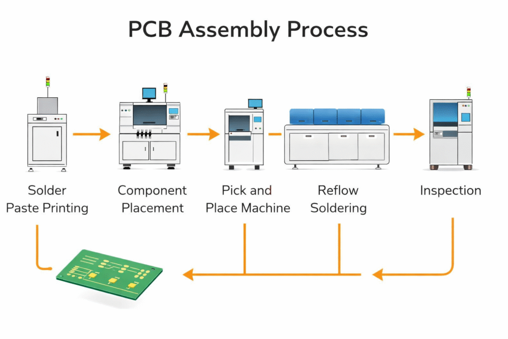
To better understand how these issues occur during production, you can refer to our PCB assembly process step-by-step guide.
What Are PCB Assembly Defects?
PCB assembly defects refer to any imperfections that occur during the process of mounting and soldering components onto a printed circuit board. These defects can affect:
- Electrical connectivity
- Mechanical strength
- Thermal performance
- Long-term reliability
Some defects are visible under optical inspection, while others remain hidden inside solder joints or beneath components, only becoming evident after deployment.
Even a microscopic defect in a solder joint can compromise the entire product, especially in applications where stability and durability are essential.
For more detailed industry guidance, refer to IPC standards for PCB assembly quality.
Why PCB Assembly Defects Occur
PCB assembly defects are rarely caused by a single factor. In most cases, they result from a combination of issues across materials, processes, design, and equipment.
1. Material-Related Issues
- Oxidized component leads or PCB pads
- Low-quality or improperly stored solder paste
- Contaminated surfaces
2. Process Control Issues
- Improper solder paste printing
- Incorrect reflow temperature profiles
- Inconsistent heating or cooling rates
3. Design Limitations
- Poor pad design or imbalance
- Insufficient spacing between components
- Lack of design for manufacturability (DFM)
4. Equipment and Calibration
- Misaligned pick-and-place machines
- Worn or contaminated nozzles
- Inaccurate vision systems
5. Human and Operational Factors
- Improper handling
- Inconsistent rework practices
- Lack of standardized procedures
In real production environments, defects often occur when multiple small deviations combine rather than from a single obvious failure.
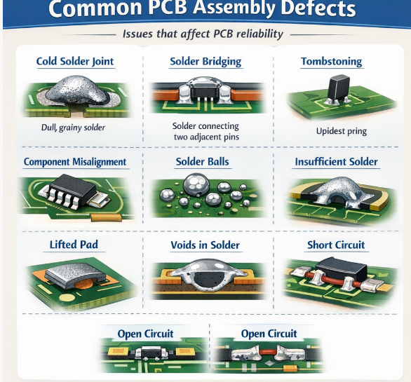
10 Common PCB Assembly Defects and How to Fix Them
PCB assembly defects can significantly impact product performance and reliability.
Below is a quick overview of the most common defects, their causes, and how to fix them.
🔹 Quick Overview of Common PCB Assembly Defects
| Defect | Typical Appearance | Main Cause | Risk Level | Fix Strategy |
|---|---|---|---|---|
| Cold Solder Joint | Dull, rough, weak joint | Low temperature / oxidation | High | Reflow + process optimization |
| Solder Bridging | Solder connecting pins | Excess solder paste | High | Remove solder + adjust stencil |
| Tombstoning | Component stands upright | Uneven heating | Medium | Rebalance heating + redesign pads |
| Solder Balling | Small solder spheres | Moisture / contamination | Medium | Clean + adjust reflow |
| Insufficient Solder | Small or incomplete joint | Poor paste printing | Medium | Improve printing process |
| Component Misalignment | Shifted or rotated parts | Placement inaccuracy | Medium | Reposition + calibrate machine |
| Lifted Pads | Pad detached from PCB | Excess heat / stress | High | Repair or replace PCB |
| Voids in Solder | Air pockets inside joint | Outgassing | Medium | Optimize reflow + design |
| Open Circuits | No electrical connection | Poor soldering | High | Re-solder + inspect |
| Short Circuits | Unintended connection | Solder bridge / debris | High | Remove short + clean |
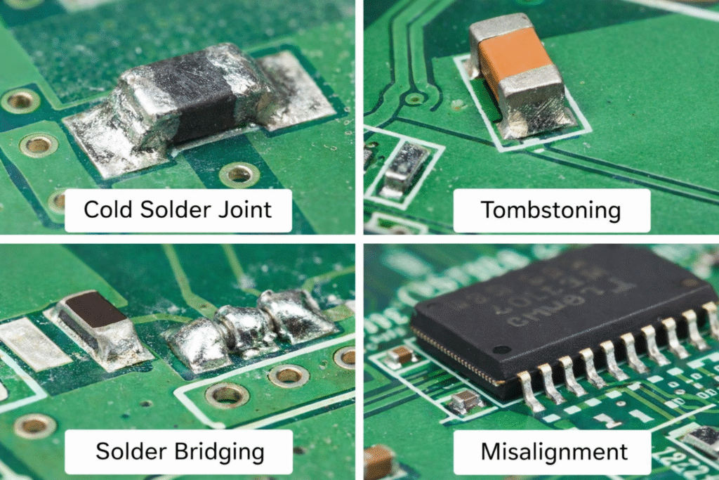
1. Cold Solder Joint
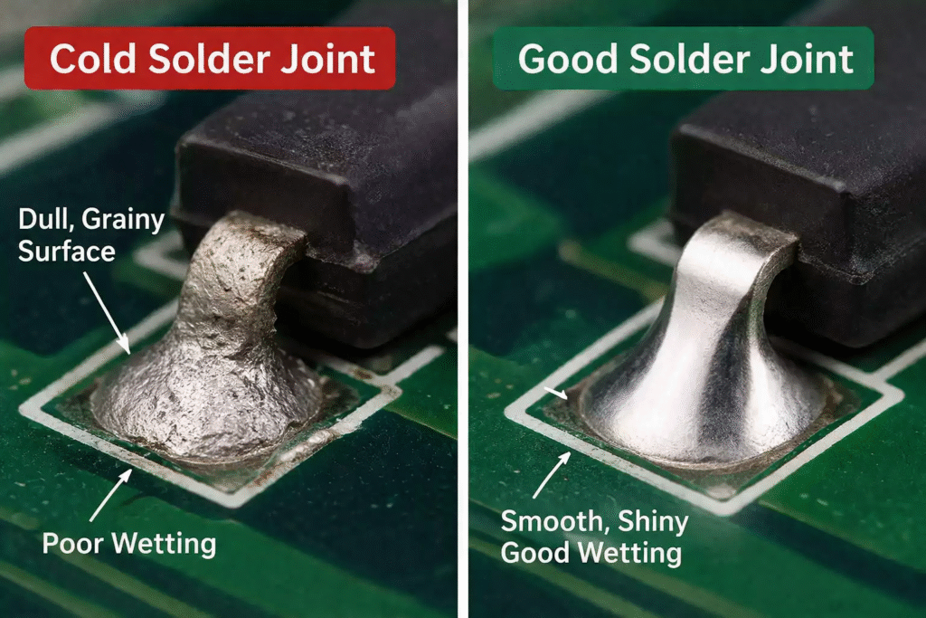
What it is:
A cold solder joint occurs when the solder does not fully melt or fails to form a proper metallurgical bond between the component lead and the PCB pad.
How it appears:
- Dull, grainy, or rough surface
- Poor wetting and uneven spread
- Weak mechanical connection
Main causes:
- insufficient reflow temperature or time due to an improper reflow soldering profile
- Oxidized surfaces
- Low solder paste activity
- Uneven heating during manual soldering
Impact:
Cold solder joints are highly unreliable. They may pass initial testing but fail under vibration, temperature changes, or long-term use.
How to fix it:
- Reheat and reflow the solder joint properly
- Adjust reflow temperature profile (peak temperature and soak time)
- Replace degraded or expired solder paste
- Clean oxidized pads or leads before soldering
Prevention:
- Optimize reflow profiles
- Ensure proper solder paste storage and handling
- Maintain clean and oxidation-free surfaces
2. Solder Bridging
What it is:
Solder bridging occurs when excess solder creates an unintended connection between adjacent pads or component leads.
How it appears:
- Visible solder connection between pins
- Common in fine-pitch ICs
Main causes:
- Excess solder paste
- Improper stencil design
- Component misalignment
- Poor solder paste printing control
Impact:
This defect leads directly to short circuits, potentially causing complete product failure or damage to components.
How to fix it:
- Remove excess solder using solder wick or rework tools
- Reinspect for complete joint integrity
- Adjust stencil aperture design
- Improve printing parameters
Prevention:
- Control solder paste volume
- Use optimized stencil designs
- Improve placement accuracy
3. Tombstoning
What it is:
A defect where one end of a small chip component lifts off the PCB, leaving the component standing upright.
How it appears:
- One side soldered, the other side lifted
- Common in small passive components (0201, 0402)
Main causes:
- Uneven heating between pads
- Imbalanced solder paste volume
- Asymmetric pad design
Impact:
The component becomes electrically disconnected, leading to circuit failure.
How to fix it:
- Remove and re-place the component
- Balance solder paste deposition
- Adjust reflow heating profile
Prevention:
- Ensure symmetric pad design
- Improve thermal balance during reflow
- Control paste printing consistency
4. Solder Balling
What it is:
Small spherical solder particles scattered around solder joints.
How it appears:
- Tiny solder balls around components
- Often near pads or under components
Main causes:
- Moisture in solder paste
- Contaminated PCB surfaces
- Rapid temperature rise during reflow
Impact:
Solder balls may cause intermittent short circuits if they move or detach.
How to fix it:
- Clean affected areas
- Adjust reflow profile
- Replace contaminated solder paste
Prevention:
- Control humidity and storage conditions
- Clean PCB surfaces
- Use proper reflow heating curves
5. Insufficient Solder
What it is:
A condition where there is not enough solder to form a reliable joint.
How it appears:
- Small or incomplete solder fillet
- Poor coverage on leads
Main causes:
- Inadequate stencil aperture
- Poor solder paste transfer
- Uneven printing
Impact:
Weak joints that may fail mechanically or electrically over time.
How to fix it:
- Add solder through rework
- Adjust stencil design
- Optimize printing process
Prevention:
- Monitor solder paste deposition volume
- Use SPI inspection systems
6. Component Misalignment
What it is:
Components are not correctly positioned on the PCB pads.
How it appears:
- Shifted or rotated components
- Uneven alignment
Main causes:
- Pick-and-place inaccuracies
- Poor PCB positioning
- Solder paste slumping
Impact:
Leads to poor solder joints, shorts, or open connections.
How to fix it:
- Remove and reposition components
- Recalibrate placement machines
- Inspect vision alignment systems
Prevention:
- Maintain equipment calibration
- Improve placement accuracy
- Verify PCB alignment systems
7. Lifted Pads
What it is:
PCB pads detach from the board surface.
How it appears:
- Pads lifted or missing
- Visible damage to PCB surface
Main causes:
- Excessive heat during rework
- Weak PCB material adhesion
- Mechanical stress
Impact:
Severe defect that may require PCB replacement or complex repair.
How to fix it:
- Repair using jumper wires (if possible)
- Replace the PCB in critical cases
- Reduce thermal stress during rework
Prevention:
- Control rework temperature and duration
- Use high-quality PCB materials
8. Voids in Solder Joints
What it is:
Air pockets trapped inside solder joints.
How it appears:
- Not visible externally
- Detected using X-ray inspection
Main causes:
- Outgassing during reflow
- Improper solder paste composition
- Poor pad design
Impact:
Reduces thermal conductivity and mechanical strength.
How to fix it:
- Adjust reflow profile
- Use appropriate solder paste
- Optimize pad design
Prevention:
- Improve thermal profile control
- Use X-ray inspection for critical components
9. Open Circuits
What it is:
Incomplete electrical connections where continuity is lost.
How it appears:
- No electrical connection between pads and leads
Main causes:
- Poor solder joints
- Misaligned components
- Broken traces
Impact:
Functional failure of the circuit.
How to fix it:
- Re-solder affected joints
- Inspect for underlying PCB issues
- Replace faulty components
Prevention:
- Improve inspection processes (AOI, ICT)
- Ensure proper solder joint formation
10. Short Circuits
What it is:
Unintended electrical connections between conductive elements.
How it appears:
- Electrical failure on power-up
- Overcurrent or overheating
Main causes:
- Solder bridging
- Conductive debris
- Tight component spacing
Impact:
Can damage components or render the board unusable.
How to fix it:
- Locate and remove the short
- Replace damaged components
- Reinspect entire circuit
Prevention:
- Improve cleanliness and inspection
- Optimize PCB layout spacing
- Enhance process control
How to Prevent PCB Assembly Defects in Mass Production
Preventing defects is always more efficient and cost-effective than repairing them.
Key strategies include:
- Implementing Design for Manufacturability (DFM)
- Controlling solder paste printing quality
- Optimizing reflow soldering profiles
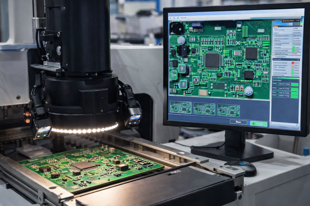
- Using inspection systems such as AOI and X-ray is essential for detecting PCB assembly defects early, as widely explained in electronics manufacturing inspection guidelines.
- Maintaining equipment calibration and consistency
A stable and repeatable manufacturing process is the foundation of high product yield.
🔹 Root Cause vs Solution Mapping
| Root Cause Category | Typical Defects | Recommended Action |
|---|---|---|
| Solder Paste Issues | Bridging, Balling, Insufficient Solder | Optimize stencil + storage |
| Reflow Profile Issues | Cold joints, Voids, Tombstoning | Adjust temperature curve |
| Placement Accuracy | Misalignment, Tombstoning | Calibrate pick-and-place |
| PCB Design Issues | Voids, Tombstoning, Shorts | Improve DFM design |
| Handling & Rework | Lifted pads, damage | Standardize rework process |
Why Process Control Matters More Than Rework
Rework can fix individual defects, but it cannot guarantee long-term reliability.
In high-volume production, relying on rework increases:
- Labor costs
- Cycle time
- Risk of secondary defects
A well-controlled process minimizes defects at the source rather than correcting them afterward.
Choosing the right manufacturing partner also plays a critical role, as explained in our guide to choosing an EMS supplier.
Conclusion
PCB assembly defects are one of the most critical factors affecting product quality in electronics manufacturing.
While defects such as cold solder joints, solder bridging, and component misalignment are common, they are largely preventable through proper design, process control, and inspection.
The key is not just identifying defects—but understanding their root causes and implementing systematic solutions to eliminate them.
FAQ
Q1: What is the most common PCB assembly defect?
Cold solder joints are among the most common and often the most difficult to detect.
Q2: Can all PCB defects be repaired?
Not all defects can be fully repaired. Some, like lifted pads, may require board replacement.
Q3: How are PCB defects detected?
Common methods include AOI (Automated Optical Inspection), X-ray inspection, and functional testing.
Q4: How can PCB assembly defects be reduced?
By improving design, controlling processes, and implementing strict quality inspection systems.
Looking for a Reliable PCB Assembly Partner?
Reducing PCB assembly defects is not just about fixing problems—it’s about preventing them through proper process control, engineering support, and manufacturing experience.
At CINDY MOULD, we provide integrated electronics manufacturing solutions, helping customers improve product quality, reduce defects, and achieve stable mass production.
If you’re looking for a reliable partner for your next project, feel free to contact us to discuss your requirements.