Cold Solder Joint PCB: Causes, Detection, Repair, and Prevention

A cold solder joint PCB defect forms when solder fails to melt, flow, or wet the PCB pad and component lead correctly. Instead of creating a stable metallurgical connection, the solder joint remains partially bonded, mechanically weak, or electrically unreliable.

Some cold solder joints are easy to recognize because they appear dull, rough, or irregular. Others look acceptable during inspection and even pass initial functional testing. The failure may only appear later when the finished product experiences vibration, thermal cycling, mechanical stress, or repeated power operation.

This makes cold solder joints particularly dangerous in electronics manufacturing. A single weak connection can cause intermittent operation, signal instability, unexplained resets, or complete product failure.

Understanding the causes of cold solder joint PCB defects is important, but manufacturers also need reliable methods for detection, repair, rework evaluation, and long-term prevention.


What Is a Cold Solder Joint in PCB Assembly?

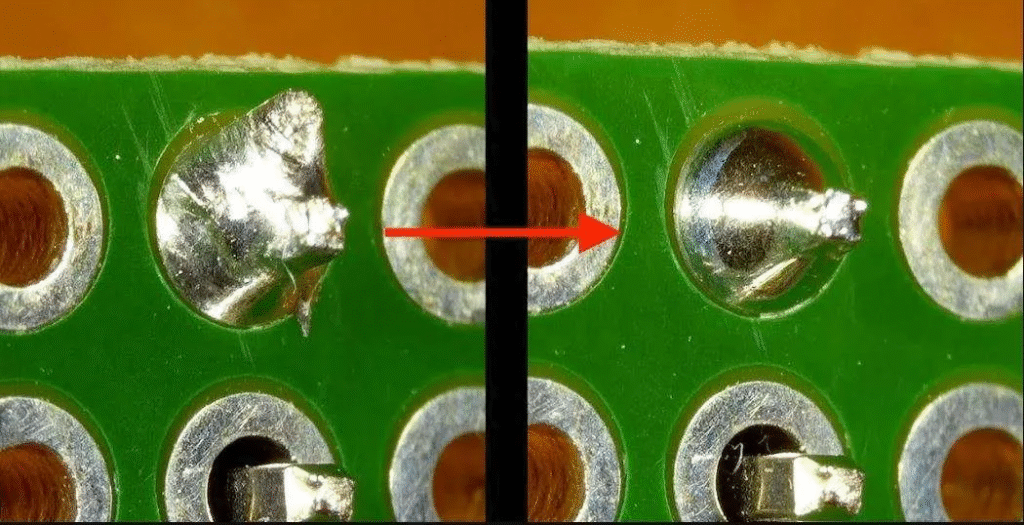
cold solder joint PCB vs good solder joint comparison

A reliable solder joint requires the solder to wet both the PCB pad and the component termination. During reflow or manual soldering, sufficient thermal energy must be applied so that the solder melts completely and forms a stable metallurgical bond.

A cold solder joint develops when this process is incomplete.

Typical characteristics include:

  • Dull, frosted, or grainy appearance
  • Rough or uneven solder surface
  • Incomplete wetting around the pad or lead
  • Irregular solder fillet shape
  • Cracks around the component termination
  • Weak mechanical attachment
  • Unstable electrical continuity

However, appearance alone cannot confirm every defect. Lead-free solder joints may naturally appear less shiny than traditional tin-lead joints, while some defective joints may still look normal from the outside.

Inspection therefore needs to consider joint geometry, wetting behavior, electrical performance, process history, and the reliability requirements of the finished product.

Solder joint acceptance should be evaluated according to applicable IPC-A-610 requirements and the product’s defined acceptance class.


Why Cold Solder Joints Are a Serious Reliability Risk

A cold solder joint is not merely a cosmetic defect. It can affect electrical performance, mechanical strength, production yield, and long-term product reliability.

Intermittent Electrical Failures

Cold solder joints may maintain electrical contact under stable conditions but lose continuity when the PCB is exposed to:

  • Mechanical vibration
  • Thermal expansion and contraction
  • Connector insertion forces
  • Enclosure assembly stress
  • Repeated power cycling

This creates intermittent failures that are difficult to reproduce. A product may pass factory testing and then fail unpredictably after shipment.

Increased Electrical Resistance

Incomplete bonding can introduce additional resistance at the connection point. Depending on the circuit, this may cause:

  • Voltage drops
  • Unstable signals
  • Timing errors
  • Localized heating
  • Reduced power efficiency
  • Inconsistent sensor readings

In low-current signal circuits, a small change in resistance may be enough to affect product behavior without creating an obvious open circuit.

Reduced Mechanical Strength

A properly formed solder joint helps secure the component termination to the PCB. A cold solder joint has lower mechanical strength and may crack during:

  • Transportation
  • Product assembly
  • Vibration testing
  • Connector operation
  • Long-term field use

The risk becomes greater when components are large, heavy, or positioned near mechanically stressed areas of the PCB.

Hidden Field Failures

The most expensive solder joint problems are often those that escape production inspection. These failures can increase:

  • Customer complaints
  • Product returns
  • Warranty costs
  • Troubleshooting time
  • Replacement expenses
  • Damage to supplier credibility

Preventing cold solder joints is therefore more valuable than relying on final inspection or repair alone.


Common Symptoms of a Cold Solder Joint PCB

Cold solder joint symptoms vary depending on the circuit and operating environment. Common warning signs include:

  • A device works only when the PCB is pressed or moved
  • The product resets during vibration
  • A signal appears and disappears intermittently
  • An LED flickers without a clear electrical cause
  • A connector works only at certain angles
  • The product passes one test cycle but fails another
  • Failure appears after heating or cooling
  • Continuity changes when the board is flexed
  • A component termination looks rough or incompletely wetted

These symptoms do not automatically prove that a cold solder joint is present, but they indicate that solder joint integrity should be investigated.


Main Causes of Cold Solder Joint PCB Defects

Cold solder joints usually result from a combination of thermal, material, equipment, design, and handling factors.

1. Insufficient Thermal Energy

Solder must reach the correct temperature and remain molten long enough to wet the relevant metal surfaces.

If the temperature is too low or the heating time is too short:

  • Solder may not melt completely
  • Flux may not activate effectively
  • Wetting may remain incomplete
  • A stable intermetallic bond may not form

Insufficient heat can occur during reflow soldering, wave soldering, selective soldering, or manual rework.

2. Incorrect Reflow Temperature Profile

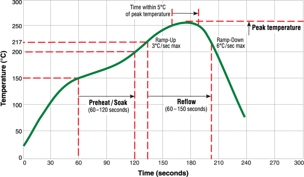
reflow soldering profile affecting cold solder joint PCB formation

Every PCBA has a different thermal response. Board thickness, copper distribution, component mass, surface finish, and component density all affect how heat moves through the assembly.

An unsuitable reflow profile may cause:

  • Uneven heating across the PCB
  • Insufficient soak time
  • Low peak temperature
  • Inadequate time above liquidus
  • Excessively rapid cooling
  • Large temperature differences between components

A profile that works for one PCB should not automatically be reused for another product without validation.

3. Oxidized PCB Pads or Component Leads

Oxidation prevents molten solder from wetting the metal surface correctly.

Common causes include:

  • Excessive material storage time
  • Damaged moisture-barrier packaging
  • Exposure to high humidity
  • Poor inventory rotation
  • Contaminated component terminations
  • Degraded PCB surface finishes

Increasing the soldering temperature may not solve severe oxidation and can introduce additional thermal damage.

4. Contamination on the Soldering Surface

Dust, oil, fingerprints, cleaning residue, and other contaminants can create a barrier between the solder and the base metal.

Possible contamination sources include:

  • Improper PCB handling
  • Unclean production fixtures
  • Poor storage conditions
  • Residue from previous processes
  • Incorrect cleaning materials
  • Manual contact with pads or leads

Clean handling and controlled storage are essential for reliable solderability.

5. Inadequate or Degraded Flux

Flux removes surface oxidation and helps molten solder spread across the pad and component termination.

Problems may occur when:

  • Flux activity is insufficient
  • Solder paste has expired
  • Paste has been stored incorrectly
  • Paste remains at room temperature for too long
  • Flux quantity is inconsistent
  • The selected flux is unsuitable for the materials

Solder paste storage, preparation, printing, and usage time must all be controlled.

6. Movement During Solidification

The component and PCB must remain stable while the solder joint cools.

Movement caused by conveyor vibration, unstable fixtures, manual handling, or component displacement can disturb the joint before solidification is complete. This may create an irregular internal structure or visible cracking.

7. Inconsistent Solder Paste Printing

Insufficient or uneven solder paste can reduce the amount of material available to form a reliable joint.

Solder paste printing parameters directly influence solder volume and joint consistency.

Printing problems may be caused by:

  • Blocked stencil apertures
  • Incorrect stencil thickness
  • Poor stencil-to-board contact
  • Inconsistent squeegee pressure
  • PCB warpage
  • Incorrect pad or aperture design

Solder paste inspection can identify many of these risks before components enter the reflow oven.

8. Manual Soldering Variation

Manual soldering depends heavily on operator technique.

Common mistakes include:

  • Incorrect iron temperature
  • Insufficient heating time
  • Heating only the solder rather than the joint
  • Using an unsuitable tip
  • Applying too much or too little solder
  • Moving the component during cooling
  • Reworking the same pad repeatedly

Temperature-controlled tools, standardized work instructions, and operator training are necessary for consistent results.

9. Poor Pad or Thermal Design

PCB design can make certain joints difficult to heat evenly.

Examples include:

  • Pads connected directly to large copper areas
  • Inconsistent thermal relief design
  • Pad dimensions that do not match the component
  • Uneven copper distribution
  • Components with very different thermal masses placed together
  • Insufficient spacing for inspection and rework

These conditions create thermal imbalance and narrow the acceptable soldering process window.


How to Detect Cold Solder Joint PCB Defects

No single inspection method can identify every cold solder joint. Effective detection combines inspection, testing, and process data.

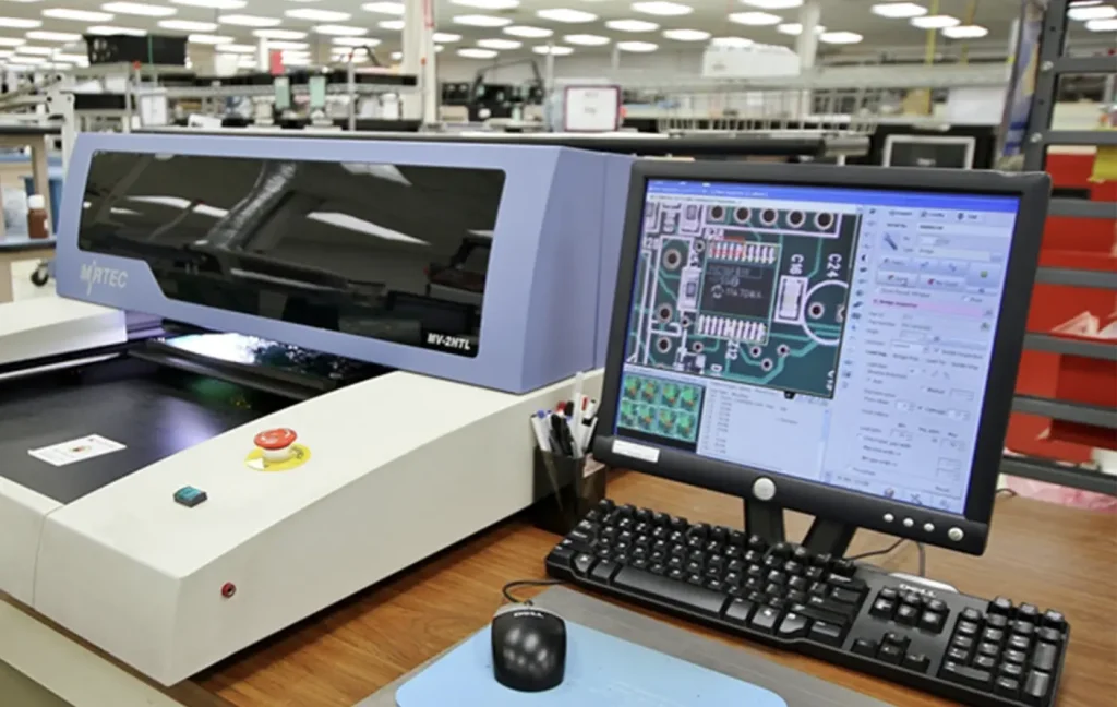
AOI inspection machine used for PCB solder joint inspection

Visual Inspection

Visual inspection can identify:

  • Rough or grainy surfaces
  • Incomplete solder fillets
  • Cracks
  • Component movement
  • Insufficient wetting
  • Obvious solder-volume problems

Magnification and controlled lighting improve inspection accuracy. However, visual inspection cannot confirm the internal metallurgical condition of every joint.

Automated Optical Inspection

AOI systems compare solder joint geometry, component position, polarity, and visible surface features against programmed criteria.

AOI is useful for detecting:

  • Irregular joint shapes
  • Insufficient solder
  • Component displacement
  • Bridging
  • Missing components
  • Visible wetting problems

AOI cannot directly measure bond strength or fully inspect hidden joints beneath components.

X-Ray Inspection

X-ray inspection is useful for BGAs, QFNs, bottom-terminated components, and other joints that cannot be examined visually.

It can reveal:

  • Voids
  • Insufficient solder coverage
  • Bridging beneath components
  • Misalignment
  • Abnormal internal joint structures

X-ray results should be interpreted together with process requirements and component specifications.

Electrical and Functional Testing

Continuity tests, in-circuit testing, and functional testing can identify unstable connections.

For intermittent failures, additional techniques may include:

  • Controlled board flexing
  • Thermal cycling
  • Vibration testing
  • Repeated power cycling
  • Monitoring resistance under stress

Testing should reproduce the conditions under which the failure occurs without damaging the product or masking the original defect.


How to Repair a Cold Solder Joint PCB

Cold solder joint PCB repair must restore both electrical continuity and mechanical reliability. Simply applying additional solder is not always sufficient.

Controlled soldering and rework procedures should follow applicable IPC J-STD-001 process requirements.

Method 1: Controlled Reheating

Controlled reheating may be suitable when:

  • The joint has minor wetting problems
  • The pad and component lead are not damaged
  • Oxidation is limited
  • The existing solder volume is adequate

The joint should be heated evenly until the solder fully reflows. It must then remain stationary during cooling.

Reheating should not be used repeatedly when the root cause is contamination, severe oxidation, or damaged materials.

Method 2: Remove and Re-Solder the Joint

Complete re-soldering is more appropriate when:

  • Existing solder is contaminated
  • Wetting is severely incomplete
  • The joint has visible cracks
  • The solder volume is unsuitable
  • Simple reheating does not restore the connection

A controlled process normally includes:

  1. Remove the existing solder.
  2. Inspect the PCB pad and component termination.
  3. Clean the area using an approved method.
  4. Apply the appropriate flux.
  5. Add fresh solder.
  6. Heat the pad and lead evenly.
  7. Allow the joint to cool without movement.
  8. Inspect and test the repaired connection.

Method 3: Replace the Component

Component replacement may be necessary when:

  • The termination is heavily oxidized
  • The component has been thermally damaged
  • Leads are deformed
  • The component has already undergone excessive rework
  • Internal component reliability is uncertain

Replacing a component costs more than reheating a joint, but it may be the safer option for high-reliability products.


When Should a PCB Be Reworked or Scrapped?

Not every cold solder joint should be repaired. The decision depends on defect severity, product requirements, PCB condition, and rework history.

ConditionRecommended action
One localized defect with an undamaged padControlled rework
Minor incomplete wettingReheat or re-solder after evaluation
Contaminated solder or severe oxidationRemove, clean, and re-solder
Damaged PCB padEngineering evaluation or scrap
Lifted trace or damaged laminateScrap or approved specialist repair
Multiple similar defects across one PCBInvestigate the process before rework
Repeated rework on the same jointConsider component or PCB replacement
Safety-critical or highly regulated productFollow approved rework limits and acceptance criteria

A board should not automatically be accepted simply because electrical continuity has been restored. The repaired area must meet the applicable acceptance, cleanliness, mechanical, and functional requirements.


Risks of Repeated Cold Solder Joint Repair

Repeated rework exposes the PCB and component to additional thermal and mechanical stress.

Possible consequences include:

  • Lifted pads
  • Damaged traces
  • PCB delamination
  • Component degradation
  • Reduced pad adhesion
  • Excessive intermetallic growth
  • Flux residue
  • Lower long-term reliability

Manufacturers should define the maximum permitted number of rework cycles according to the PCB construction, component sensitivity, product requirements, and approved process documentation.


How to Prevent Cold Solder Joint PCB Defects

Prevention requires control across design, materials, equipment, process parameters, and inspection.

Develop a Product-Specific Reflow Profile

A reflow profile should be validated using thermocouples placed at representative thermal locations.

The validation should consider:

  • PCB thickness
  • Copper distribution
  • Component thermal mass
  • Solder paste requirements
  • Peak temperature
  • Soak duration
  • Time above liquidus
  • Heating and cooling rates

Profiling should reflect actual production conditions rather than an isolated engineering trial.

Control Solder Paste Handling

Important controls include:

  • Refrigerated storage according to supplier instructions
  • Controlled return to room temperature
  • Shelf-life monitoring
  • Time-out-of-refrigeration limits
  • Proper mixing where required
  • First-in, first-out inventory management
  • Prevention of contamination

Expired or improperly handled solder paste should not be used to avoid material waste.

Improve PCB and Component Storage

PCBs and components should be protected from humidity, oxidation, and contamination.

Recommended controls include:

  • Sealed packaging
  • Humidity indicators where applicable
  • Controlled storage conditions
  • Moisture-sensitivity management
  • Traceable material lots
  • Defined exposure limits

Material condition should be verified before production begins.

Monitor Solder Paste Printing

Printing is one of the most important upstream controls in SMT assembly.

Manufacturers should monitor:

  • Paste volume
  • Deposit height
  • Aperture release
  • Stencil cleanliness
  • Alignment
  • Squeegee parameters
  • PCB support and flatness

Solder paste inspection allows corrective action before defective boards continue through placement and reflow.

Maintain Stable Equipment Conditions

Production equipment should be calibrated and maintained according to a defined schedule.

Important areas include:

  • Oven-zone temperature
  • Conveyor speed
  • Soldering iron temperature
  • Rework-station calibration
  • Fixture stability
  • Exhaust and airflow conditions
  • Inspection equipment accuracy

Small equipment deviations can create recurring defects across an entire production batch.

Apply PCB Design for Manufacturability

DFM reviews should examine:

  • Pad dimensions
  • Thermal relief
  • Copper balance
  • Component spacing
  • Stencil aperture design
  • Accessibility for inspection
  • Accessibility for rework
  • Component orientation

A manufacturable design provides a wider and more stable soldering process window.

Standardize Manual Soldering and Rework

Manual operations should follow documented procedures covering:

  • Approved tools and materials
  • Temperature limits
  • Heating duration
  • Flux selection
  • Cleaning requirements
  • Inspection criteria
  • Rework limits
  • Operator qualification

Repair results should not depend only on individual operator experience.

Track Defects and Rework Data

A rising rework rate is often a sign of upstream process instability.

Useful data includes:

  • Defect type
  • Component reference
  • PCB location
  • Production batch
  • Material lot
  • Equipment line
  • Reflow profile
  • Operator or workstation
  • Repair method
  • Retest result

Repeated defects in the same location may indicate pad-design, stencil, placement, or thermal-balance problems rather than random workmanship variation.

Reviewing other common PCB assembly defects can also help distinguish isolated workmanship issues from broader process instability.


Cold Solder Joint PCB vs Good Solder Joint

Inspection factorGood solder jointCold solder joint
WettingComplete wetting of pad and terminationPartial or incomplete wetting
SurfaceConsistent with the solder alloy and processOften rough, grainy, or irregular
Fillet shapeControlled and properly formedUneven or poorly formed
Electrical behaviorStableMay be intermittent or resistive
Mechanical strengthSuitable for the applicationWeak or vulnerable to cracking
ReliabilityPredictable under validated conditionsUncertain under vibration or thermal stress

Surface appearance should always be evaluated according to the solder alloy and applicable acceptance requirements. A shiny surface alone does not guarantee a reliable joint.


Real Manufacturing Scenario

A product may perform normally during prototype builds because technicians manually correct soldering problems and production volumes are low.

When production increases, several small variations may occur simultaneously:

  • Solder paste remains on the line longer
  • Oven loading changes
  • PCB thermal conditions become less uniform
  • Material lots vary
  • Operators perform more rework
  • Inspection criteria are applied inconsistently

The result may be a gradual increase in intermittent failures rather than an obvious production shutdown.

Repairing individual joints may restore the affected boards, but it does not solve the underlying problem. The manufacturer must compare defect locations, material lots, printing data, reflow profiles, and rework records to identify the common cause.

The objective is not simply to repair every defective joint. It is to prevent the same defect from recurring in subsequent production batches.


Frequently Asked Questions

What does a cold solder joint look like?

It may appear dull, rough, cracked, irregular, or incompletely wetted. However, appearance varies by solder alloy, so visual inspection should be supported by testing and process evaluation.

Can a cold solder joint pass functional testing?

Yes. A cold solder joint may maintain temporary electrical contact and pass initial testing before failing under vibration, thermal cycling, or mechanical stress.

Can a cold solder joint be repaired?

Yes, if the PCB pad, component termination, and surrounding materials remain undamaged. Repair may involve controlled reheating, removal and re-soldering, or component replacement.

Is reheating a cold solder joint enough?

Reheating may correct a minor defect, but it is unsuitable when the solder is contaminated, the surfaces are oxidized, or the pad or component has been damaged.

How many times can a solder joint be reworked?

There is no universal number for every PCB. Rework limits should be defined according to the PCB construction, component sensitivity, product reliability requirements, and approved manufacturing procedure.

Can AOI detect every cold solder joint?

No. AOI can identify visible shape and wetting abnormalities, but it cannot directly confirm internal metallurgical bonding or inspect every hidden connection.

Can repaired solder joints be reliable?

A properly controlled repair can restore reliability when the materials are undamaged and the joint meets inspection and testing requirements. Repeated or poorly controlled rework can reduce PCB lifespan.


Conclusion

Cold solder joint PCB defects are caused by more than insufficient heat alone. Reflow-profile errors, oxidation, contamination, degraded flux, solder-paste printing problems, movement during cooling, manual process variation, and poor pad design can all contribute to unreliable connections.

Effective detection requires a combination of visual inspection, AOI, X-ray inspection, electrical testing, and process-data analysis. Repair methods must be selected according to the condition of the joint, PCB pad, component, and surrounding materials.

Most importantly, repair should not replace root-cause control. Stable soldering depends on product-specific thermal profiling, controlled materials, consistent printing, calibrated equipment, manufacturable PCB design, standardized rework, and traceable defect data.

By controlling these factors throughout production, manufacturers can reduce rework, prevent intermittent field failures, and improve the long-term reliability of complete electronic products.

Get a Free Quote