
Introduction

PCB Design Review Checklist is one of the most critical steps in ensuring a smooth transition from prototype to mass production. A well-executed PCB design review helps identify potential manufacturing risks early, before they turn into costly production issues.
In real production environments, many problems that appear during assembly, testing, or even after shipment can often be traced back to design-stage decisions. Issues such as soldering defects, unstable connections, or inconsistent product performance are rarely random — they are usually the result of overlooked details during design review.
Whether you are working on a new product or scaling an existing design, overlooking key aspects can lead to delays, rework, and increased costs. This is especially true when moving from prototype to mass production, where small design variations can quickly become large-scale problems.
This article provides a practical PCB Design Review Checklist with 10 critical items that engineers and manufacturers should verify before production. By following this checklist, you can significantly reduce risks, improve product reliability, and ensure a more stable manufacturing process.
1. BOM (Bill of Materials) Review: Ensure Accuracy and Availability
As part of any PCB Design Review Checklist, BOM verification is one of the first and most critical steps.
A comprehensive and accurate Bill of Materials (BOM) ensures that all required components are correctly specified and available for production. However, in many projects, BOM issues are a major source of delays and unexpected changes.
For example, missing part numbers, outdated component versions, or components with long lead times can stop production entirely. In many cases, these issues can directly impact production yield in electronics manufacturing, leading to increased rework, delays, and inconsistent product quality.
Key Points to Check:
- Component specifications match design requirements
- Approved suppliers and lead times are confirmed
- Quantities are aligned with production volume
Example BOM Review Checklist
| Check Item | Description | Key Considerations |
|---|---|---|
| Part Number | Ensure all part numbers match design files | Cross-check with supplier data |
| Supplier Information | Confirm supplier availability and lead time | Avoid long lead-time components |
| Quantity | Verify component quantities for production | Match batch size requirements |
By validating the BOM early, you reduce procurement risks and ensure a smoother production flow.
2. Gerber Files and Design File Consistency
In any PCB Design Review Checklist, verifying Gerber file accuracy is essential.
Gerber files are the direct input for PCB fabrication. Even a small mismatch between design files and Gerber outputs can result in incorrect board dimensions, missing layers, or drilling errors.
In practice, version control is a common issue. Teams may accidentally send outdated files to manufacturers, leading to production based on incorrect data.
Key Points to Check:
- All layers are correctly exported
- Drill files match pad and via definitions
- File versions are consistent and up to date
Ensuring consistency between design data and manufacturing files helps prevent costly fabrication mistakes and rework.
3. PCB Layer Design: Ensure Electrical Integrity
Layer stackup design is a critical part of any PCB Design Review Checklist, especially for multi-layer boards.
Improper layer design can lead to signal interference, power instability, and electromagnetic issues. These problems may not always appear during initial testing but can affect long-term performance.
For example, an incomplete ground plane may introduce noise, while poor power distribution can cause voltage fluctuations across the board.
Key Points to Check:
- Proper separation of signal and power layers
- Continuous ground planes without breaks
- Suitable via structures for routing
Example PCB Layer Stackup Design
| Layer Type | Recommended Design | Purpose |
|---|---|---|
| Power Plane | Stable, low-noise distribution | Reduce voltage fluctuation |
| Ground Plane | Continuous and unbroken | Minimize EMI and noise |
A well-designed stackup improves both signal integrity and overall product reliability.

4. Pad Design and Sizing: Ensure Reliable Assembly
Pad design validation is a key element in any PCB Design Review Checklist to ensure consistent soldering quality.
Incorrect pad design is one of the most common causes of assembly defects. Pads that are too small may lead to weak solder joints, while oversized pads can cause solder bridging.
These issues often pass visual inspection but result in failures during operation.
Key Points to Check:
- Pad size matches component footprint
- Spacing prevents solder bridging
- Vias are not interfering with pads
Example Pad Design Table
| Component Type | Pad Size (mm) | Spacing (mm) |
|---|---|---|
| SMD | 0.3–0.6 | 0.5–1.5 |
| Through-hole | 0.8–1.2 | 1.5–2.5 |
Correct pad design ensures stable assembly and reduces defect rates in mass production.
5. Current and Voltage Load Analysis
Electrical load validation is an important part of any PCB Design Review Checklist.
If trace widths are not properly designed, excessive current can lead to overheating, which may damage components or reduce product lifespan.
In high-power applications, poor power distribution can also create uneven performance across different units.
Key Points to Check:
- Trace width supports current requirements
- Power distribution is balanced
- Heat dissipation is considered
Example Current Capacity Table
| Component Type | Trace Width (mm) | Current (A) |
|---|---|---|
| Low Power | 0.2–0.3 | 0.5–2 |
| High Power | 0.5–1.0 | 5–10 |
Proper electrical design prevents long-term reliability issues and improves consistency.
6. Routing and Trace Layout Optimization
Efficient routing is another important element in a PCB Design Review Checklist.
Poor routing increases the risk of signal interference, delays signal transmission, and complicates manufacturing. It may also lead to inconsistent performance between units.
Key Points to Check:
- Avoid unnecessary trace crossings
- Keep signal paths short and direct
- Maintain consistent routing standards
Optimized routing improves signal quality and simplifies production processes.
7. Impedance Control for High-Speed Design
A professional PCB Design Review Checklist always includes impedance verification.
High-speed signals require controlled impedance to maintain signal integrity, especially in applications where signal integrity is critical.
Key Points to Check:
- Controlled impedance (e.g., 50Ω)
- Proper differential pair routing
- Minimized via impact
This is especially critical for communication devices and high-frequency applications.
8. EMC (Electromagnetic Compatibility) Design Check
EMC validation is a necessary part of a complete PCB Design Review Checklist, especially when products need to comply with industry standards such as IPC guidelines.
Without proper EMC design, products may fail certification tests or experience unstable operation in real-world environments.
Key Points to Check:
- Continuous grounding strategy
- Shielding for sensitive areas
- Separation of power and signal traces
Addressing EMC early helps avoid redesign and compliance issues later.
9. Tolerance and Assembly Considerations
Mechanical tolerance verification is another key step in a PCB Design Review Checklist.
Even small misalignments can create assembly difficulties, increase stress on components, or lead to long-term reliability issues.
Key Points to Check:
- Component placement accuracy
- Hole and via tolerances
- Mechanical fit with enclosure
Good tolerance control ensures smooth assembly and consistent product quality.
10. DFM (Design for Manufacturability)
DFM validation is a core part of any PCB Design Review Checklist.
Designs that ignore manufacturing constraints often create challenges when moving from prototype to mass production, resulting in higher costs, longer production time, and increased defect rates.
Key Points to Check:
- Simplified routing
- Accessible component placement
- Avoid unnecessary complexity
Example DFM Checklist
| DFM Principle | Description | Benefit |
|---|---|---|
| Simplified Routing | Reduce layout complexity | Lower cost and faster production |
| Minimize Layers | Avoid unnecessary layers | Improve manufacturability |
Applying DFM principles ensures your design is production-ready.
Conclusion
By following this PCB Design Review Checklist, engineers and manufacturers can identify potential risks before production begins.
A structured design review not only improves product reliability but also reduces delays, rework, and manufacturing costs. Many issues that appear during production can be prevented entirely by addressing them during the design stage.
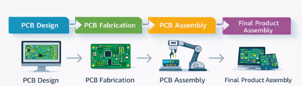
If you are preparing for production or evaluating your current design, it is also important to understand the full electronics manufacturing process from PCB assembly to final product integration to achieve a more stable and scalable manufacturing outcome.
👉 Contact CINDY Mould to get expert support from PCB design to full product assembly.