
Introduction
Cold solder joint PCB defects are among the most common causes of failure in PCB assembly, especially when products transition from prototype to mass production.
In modern electronics manufacturing, solder joint integrity directly affects electrical performance, mechanical strength, and long-term reliability. Even when high-quality components and well-designed PCBs are used, poor soldering can still introduce hidden defects that only become apparent after products reach the field.
Among various soldering defects, cold solder joints are particularly dangerous. They often pass initial inspection and electrical testing, yet lead to intermittent failures, signal instability, or premature breakdown during real-world use.
Understanding cold solder joint PCB causes and implementing effective prevention strategies is essential for ensuring stable and scalable production.
What Is a Cold Solder Joint in PCB Assembly
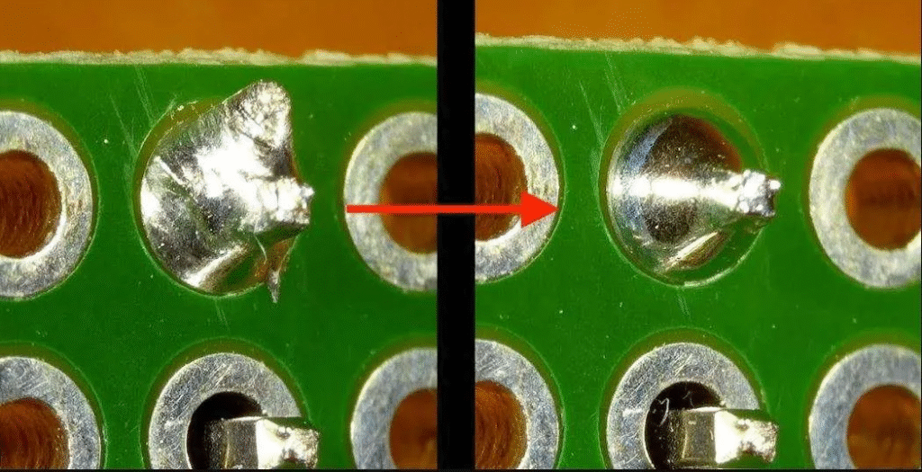
A cold solder joint is formed when solder fails to fully reflow and properly wet both the PCB pad and the component lead. Instead of forming a strong metallurgical bond, the connection remains partially fused or mechanically weak.
A properly formed solder joint creates a uniform intermetallic layer between the solder and base metals.
According to IPC standards, proper solder joint formation requires complete wetting and reliable metallurgical bonding between solder and base materials.
In contrast, a cold solder joint has an incomplete or poorly developed bonding structure.
Typical characteristics include:
- Dull, matte, or frosted appearance
- Rough or uneven surface texture
- Incomplete wetting on pads or leads
- Irregular solder fillet shape
- Micro-cracks that may not be visible without magnification
These defects significantly reduce the reliability of the connection and increase sensitivity to environmental stress.
Common Cold Solder Joint PCB Symptoms
Cold solder joints are difficult to detect because they may not immediately cause failure. However, several symptoms can indicate their presence:
- Intermittent electrical connection
- Device resets or unstable performance
- Signal distortion in high-frequency circuits
- Sudden failure after vibration or temperature change
- Products passing initial tests but failing in the field
These symptoms often lead to complex troubleshooting and increased after-sales costs.
Why Cold Solder Joints Are a Critical Reliability Risk
Cold solder joints are not cosmetic defects. They directly impact product performance and long-term stability.
Intermittent Failures in Real Use
Cold solder joints can behave normally under stable conditions but fail when exposed to:
- Mechanical vibration
- Thermal cycling
- Power on/off cycles
This unpredictability makes root cause analysis difficult.
Electrical Performance Degradation
Poor solder joints introduce higher electrical resistance, which can cause:
- Signal distortion
- Timing issues
- Reduced circuit efficiency
In precision electronics, even minor resistance variation can lead to significant performance problems.
Reduced Mechanical Strength
Cold solder joints lack structural integrity and may fail during:
- Transportation
- Assembly into enclosures
- Daily usage
This can result in cracked or completely detached connections.
Long-Term Reliability Risks
In many cases, cold solder joints are a major contributor to early-life product failure.
Failure rates can increase by 5% to 15% during mass production if process control is not properly maintained.
This leads to:
- Warranty claims
- Product returns
- Brand reputation damage
Main Causes of Cold Solder Joint PCB Defects
Cold solder joints are usually caused by a combination of process, material, and environmental factors.
Insufficient Thermal Energy
Solder must fully melt and remain molten long enough to ensure proper wetting.
If heat input is insufficient:
- Solder does not fully flow
- Wetting angles are poor
- Bonding remains incomplete
This is common when reflow peak temperature is too low or heating time is too short.
Poor Reflow Temperature Profile
A well-controlled reflow profile is critical for solder joint formation.
Typical stages include:
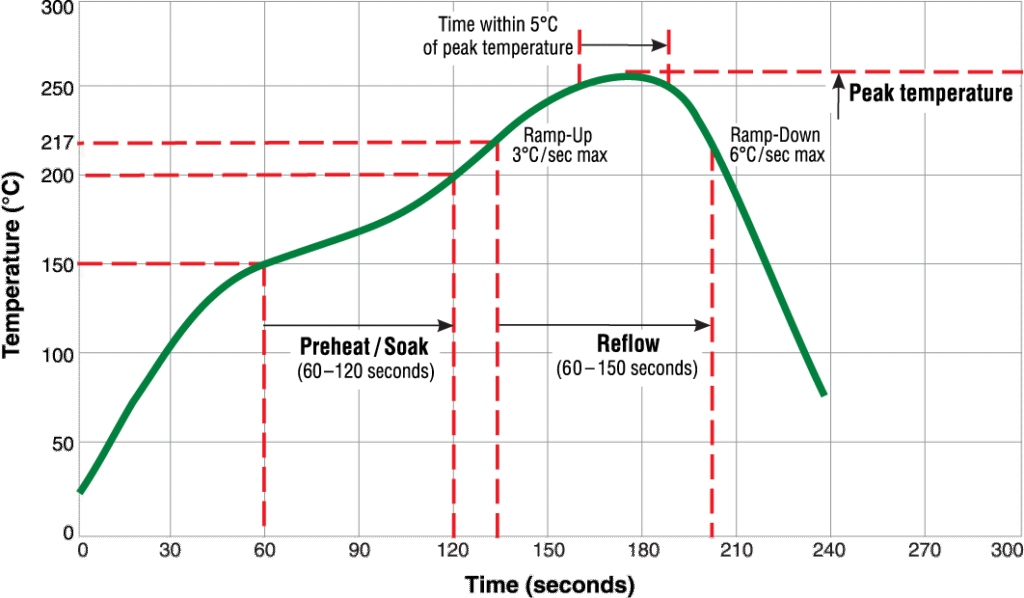
Typical reflow soldering temperature profile showing preheat, soak, reflow, and cooling stages in PCB assembly.
- Preheat
- Soak
- Reflow
- Cooling
If the profile is not optimized:
- Uneven heating occurs
- Solder may not fully melt
- Thermal imbalance develops across the PCB
For more details on optimizing reflow processes, you can refer to our guide on reflow soldering profile and its impact on PCB assembly reliability.
Oxidation of Pads or Leads
Oxidation prevents proper solder wetting.
This directly reduces solderability, which is a key factor in achieving reliable solder joints.
It is often caused by:
- Long storage time
- High humidity exposure
- Poor packaging conditions
Severely oxidized surfaces cannot form reliable solder joints even at higher temperatures.
Contamination and Surface Impurities
Contaminants act as barriers between solder and metal surfaces.
Common sources include:
- Fingerprints
- Dust
- Residual chemicals
This results in weak bonding and incomplete wetting.
Inadequate or Degraded Flux
Flux removes oxidation and promotes solder flow.
Problems occur when:
- Flux activity is insufficient
- Solder paste is degraded
- Storage conditions are improper
This leads to uneven solder spread and poor joint quality.
Movement During Cooling
Solder joints must remain stable during solidification.
Any movement caused by:
- Conveyor vibration
- Fixture instability
- Manual handling
can disrupt joint formation and create cold solder joints.
Variability in Manual Soldering
Manual soldering introduces inconsistency due to:
- Uneven heating
- Incorrect timing
- Operator skill differences
Standardization and training are essential to reduce variability.
How to Identify Cold Solder Joint PCB Issues
Accurate detection requires multiple inspection methods.
Visual Inspection
Basic visual inspection can identify surface defects but cannot detect internal bonding issues.
AOI (Automated Optical Inspection)
AOI can detect:
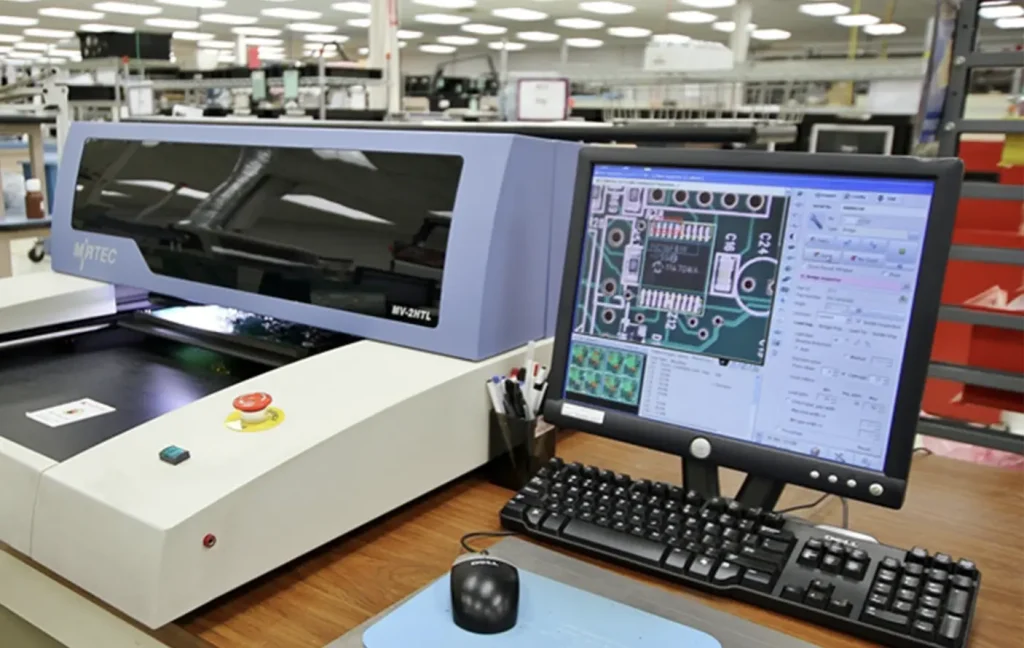
AOI inspection system used to automatically detect solder joint defects and improve quality control in PCB manufacturing.
- Shape irregularities
- Insufficient solder volume
However, it cannot evaluate metallurgical quality.
X-ray Inspection
X-ray is essential for hidden joints such as BGAs.
It reveals:
- Internal voids
- Incomplete solder coverage
Electrical Testing
Functional testing validates real-world performance.
Intermittent faults often indicate hidden solder joint problems.
How to Fix Cold Solder Joint PCB Issues
Repairing cold solder joints requires careful rework procedures.
Common methods include:
- Reheating the joint with proper temperature control
- Removing old solder and reapplying fresh solder
- Cleaning oxidized surfaces before rework
- Applying appropriate flux to improve wetting
However, repair is only a temporary solution. Preventing defects during production is far more effective.
Proven Methods to Prevent Cold Solder Joint PCB Defects
Effective prevention requires a systematic approach.
Develop Stable Reflow Profiles
- Profile each product individually
- Monitor temperature using thermocouples
- Validate under real production conditions
Control Material Storage
- Use humidity-controlled environments
- Track solder paste shelf life
- Apply FIFO inventory management
Maintain Clean Production Conditions
- Use gloves during handling
- Clean work surfaces regularly
- Implement contamination control procedures
Use High-Quality Materials
- Select reliable PCB finishes
- Source components from certified suppliers
- Use stable solder paste formulations
Optimize Flux Performance
- Ensure proper activity level
- Monitor application consistency
- Prevent flux degradation
Strengthen Process Control
- Calibrate equipment regularly
- Apply statistical process control (SPC)
- Conduct routine audits
Improve Operator Training
- Standardize work instructions
- Provide regular training
- Monitor operator performance
Apply DFM Principles Early
For a structured approach to improving manufacturability, refer to our PCB design review checklist for production readiness.
- Optimize pad design
- Ensure thermal balance
- Improve component layout
Cold Solder Joint PCB vs Good Solder Joint
Understanding the difference helps improve inspection accuracy.
| Feature | Good Solder Joint | Cold Solder Joint |
|---|---|---|
| Appearance | Smooth, shiny | Dull, rough |
| Wetting | Complete | Incomplete |
| Strength | High | Weak |
| Reliability | Stable | Unpredictable |
| Failure Risk | Low | High |
Real Manufacturing Insight
In real manufacturing environments, cold solder joint PCB issues often appear during production scale-up rather than in early prototypes.
For example, a product may pass all initial functional tests during pilot runs, but after entering mass production, failure rates suddenly increase. Investigation often reveals subtle but critical variations, such as:
- Slight deviations in reflow temperature profiles
- Differences in solder paste batches
- Environmental humidity changes on the production floor
These small inconsistencies can significantly affect solder joint formation, leading to hidden defects that only appear during field use.
Consistency across production batches is essential to maintain long-term reliability.
Frequently Asked Questions
What does a cold solder joint PCB look like
It typically appears dull, rough, or uneven, with poor wetting between solder and metal surfaces.
What causes cold solder joint PCB defects
They are caused by insufficient heat, oxidation, contamination, poor flux performance, or movement during cooling.
Can cold solder joints fail over time
Yes, they often lead to intermittent failures and long-term reliability issues.
Can AOI detect cold solder joints
AOI can detect visible defects but cannot fully evaluate internal bonding quality.
Conclusion
Cold solder joint PCB defects remain a major challenge in electronics manufacturing due to their hidden nature and long-term impact on reliability.
They are not caused by a single issue but by a combination of process, material, and environmental factors. Eliminating them requires a comprehensive approach that integrates process control, material management, and design optimization.
For manufacturers facing recurring cold solder joint PCB issues, improving process control alone may not be enough. A comprehensive approach that integrates PCB manufacturing, assembly, and final product validation is essential.
You can also explore how final assembly impacts product reliability to better understand how soldering quality affects overall product performance.
Working with an experienced manufacturing partner can help identify hidden process risks early, stabilize production, and ensure consistent product reliability across batches.
If you are encountering soldering-related failures in your projects, feel free to contact CINDY Mould for practical engineering support and manufacturing solutions.