Introduction
SMT inspection plays a critical role in ensuring quality and stability in modern electronics manufacturing. Surface Mount Technology (SMT) has become the dominant assembly method across consumer electronics, industrial equipment, automotive systems, and communication infrastructure. As production volumes increase and circuit complexity grows, structured SMT inspection processes are essential for detecting defects early and maintaining reliable assembly performance.
Although modern production lines use high-speed placement machines and automated reflow soldering equipment, production stability still depends heavily on inspection and process control. Even small variations in solder paste deposition, component alignment, or solder joint formation can lead to defects that affect electrical performance and long-term product reliability.
Typical SMT assembly defects may include:
- insufficient solder joints
- solder bridges between pads
- component misalignment
- polarity errors
- hidden solder defects beneath packages such as BGAs
If these defects are not detected early through effective SMT inspection, they may propagate through later production stages and eventually lead to product failures, expensive rework, or field reliability issues.
To control these risks, modern SMT production lines rely on layered inspection strategies that monitor different stages of the manufacturing process.
Three inspection technologies form the foundation of most SMT inspection systems:
SPI (Solder Paste Inspection)
AOI (Automated Optical Inspection)
AXI (Automated X-ray Inspection)
Each of these technologies focuses on different types of manufacturing risks. When combined, they create a comprehensive SMT inspection framework that helps maintain consistent production quality.
SMT Inspection Technologies Overview
| Inspection Method | Full Name | Inspection Stage | Main Purpose |
|---|---|---|---|
| SPI | Solder Paste Inspection | After solder paste printing | Verify solder paste volume and alignment |
| AOI | Automated Optical Inspection | After placement or reflow | Detect visible assembly defects |
| AXI | Automated X-ray Inspection | After reflow | Inspect hidden solder joints |
Together these inspection technologies form a multi-layer SMT inspection system that improves production visibility and reduces manufacturing risk.
SPI: Controlling Solder Paste Deposition
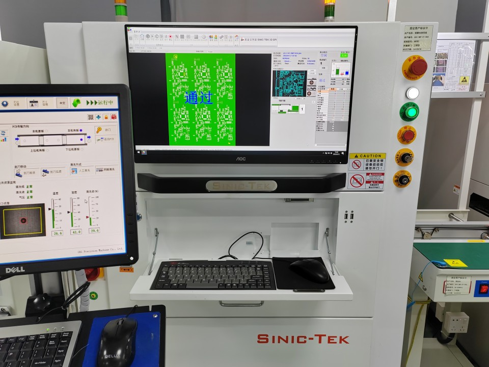
Solder Paste Inspection (SPI) is typically the first inspection step in SMT production. It takes place immediately after solder paste printing and before components are placed on the PCB.
Although solder paste printing appears to be a simple process, it is one of the most critical stages in SMT assembly. A large percentage of soldering defects originate from problems during the printing stage, which is why SPI plays a key role in early SMT inspection.
SPI systems use 3D measurement technology to evaluate several parameters related to solder paste deposition:
SPI is widely recognized in electronics manufacturing standards as a critical step in solder paste control.
As part of the PCB assembly process, SPI inspection helps ensure that solder paste deposition meets the requirements for reliable SMT production.
- solder paste volume
- paste height and thickness
- paste coverage area
- paste alignment accuracy
These measurements allow engineers to detect abnormal printing conditions early in the process.
For example, insufficient solder paste may result in weak solder joints after reflow. Excess solder paste can cause solder bridges between pads. Misaligned paste deposits may lead to component shift during placement.
When SPI detects these issues, engineers can intervene immediately by adjusting the stencil alignment, cleaning the stencil, or recalibrating the printing equipment.
Early detection through SPI inspection significantly reduces the risk of defects propagating through the rest of the assembly process.
Common SPI Defects
| Defect Type | Cause | Impact |
|---|---|---|
| Insufficient solder paste | Incomplete stencil filling | Weak solder joints |
| Excess solder paste | Excessive deposition | Solder bridges |
| Misaligned paste | Stencil alignment errors | Component shift |
| Uneven paste height | Printing pressure variation | Inconsistent solder joints |
AOI: Detecting Assembly Defects
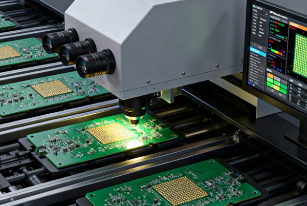
After solder paste printing and component placement, the next inspection stage is Automated Optical Inspection (AOI).
AOI systems use high-resolution cameras combined with advanced image recognition algorithms to inspect PCB assemblies. The system compares captured images with predefined reference models to detect deviations from expected assembly patterns.
AOI inspection can be performed at multiple stages in the production line.
Within a complete electronics manufacturing process, AOI inspection plays a critical role in ensuring assembly accuracy before and after reflow.
Post-placement AOI verifies whether components are positioned correctly before soldering occurs. Post-reflow AOI focuses on solder joint quality and final component alignment.
AOI systems are capable of detecting many types of assembly defects, including:
- missing components
- incorrect component orientation
- polarity errors
- component offset or rotation
- tombstoning defects
- solder bridges
- insufficient solder joints
Because AOI inspection is automated and fast, it can be integrated directly into SMT production lines. This enables manufacturers to monitor assembly quality in real time and identify problems early within the SMT inspection process.
For complex circuit boards containing hundreds or thousands of components, AOI provides consistent inspection coverage that would be difficult to achieve with manual inspection.
AXI: Inspecting Hidden Solder Joints
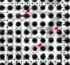
While AOI systems are highly effective at detecting visible defects, certain solder joints cannot be inspected optically.
Components such as BGAs (Ball Grid Arrays), QFNs, and other advanced packaging technologies contain solder joints hidden beneath the component body. These joints cannot be evaluated from the surface of the PCB.
To inspect these hidden connections, manufacturers rely on Automated X-ray Inspection (AXI).
AXI systems use X-ray imaging technology to visualize internal solder structures within PCB assemblies. This allows engineers to detect defects that would otherwise remain invisible during optical inspection.
X-ray inspection is widely used to evaluate hidden solder joints in advanced electronic assemblies.
Typical defects detected by AXI include:
- voids inside solder joints
- incomplete solder connections
- bridging beneath component bodies
- head-in-pillow defects
- BGA solder ball deformation
Because modern electronics designs increasingly rely on high-density packages, AXI inspection has become critical in industries such as automotive electronics, aerospace systems, and industrial control equipment.
AXI therefore provides another essential layer of verification within a complete SMT inspection strategy.
Comparison of SMT Inspection Methods
| Inspection | Detects | Limitations |
|---|---|---|
| SPI | Solder paste volume and alignment | Cannot inspect components |
| AOI | Component placement and visible solder defects | Cannot inspect hidden joints |
| AXI | Internal solder joint quality | Slower and higher equipment cost |
Each inspection technology provides unique advantages. When used together, they form a comprehensive SMT inspection strategy that significantly improves production reliability.
Building a Multi-Layer Inspection Strategy
The most effective SMT quality control systems combine SPI, AOI, and AXI into a coordinated inspection framework.
A typical SMT inspection sequence may look like this:
SPI → Placement → AOI → Reflow → AXI
Each stage focuses on different manufacturing risks.
SPI verifies solder paste deposition accuracy.
AOI detects component placement errors and visible solder defects.
AXI confirms the integrity of hidden solder joints.
By combining these technologies, manufacturers create overlapping inspection layers that greatly reduce the likelihood of defective boards progressing through the production process.
Inspection data can also be integrated into manufacturing monitoring systems to analyze defect trends and improve process stability.
Inspection as a Process Control Tool
In modern electronics manufacturing, inspection is no longer treated as a final quality checkpoint.
Instead, SMT inspection technologies are increasingly used as process control tools.
SPI, AOI, and AXI systems generate valuable production data that helps engineers monitor process stability and detect manufacturing variations early.
For example:
- SPI may detect solder paste volume variation caused by stencil wear
- AOI may reveal placement accuracy issues
- AXI may identify solder voiding related to reflow temperature profiles
By analyzing inspection data, manufacturers can adjust production parameters and maintain consistent production performance.
This data-driven approach allows manufacturers to maintain high reliability even in high-volume production environments.
Next Steps
For companies developing complex electronic products, inspection is no longer a secondary quality step — it has become an essential part of manufacturing strategy.
Understanding both SMT inspection and the box build assembly process is essential for maintaining stable production and final product quality.
When SMT inspection systems such as SPI, AOI, and AXI are integrated into the production workflow, manufacturers gain greater visibility into process stability. Instead of discovering defects during final testing or assembly, issues can be detected earlier and corrected before they propagate through the production line.
For engineering teams and procurement managers evaluating electronics manufacturing partners, understanding the SMT inspection capabilities of a supplier can provide valuable insight into their process control maturity.
Many companies begin by reviewing how inspection is implemented across the SMT production line — from solder paste verification to final solder joint validation.
If you are evaluating manufacturing readiness for a new electronics product or reviewing inspection coverage in an existing production program, an early technical discussion with an experienced manufacturing team can help clarify potential risks before production begins.
For an initial conversation, see Contact CINDY Mould.