In electronics projects, PCB and PCBA are tossed around interchangeably all the time—and honestly, I get why. They sound almost identical, and when you’re staring at a finished board, it’s easy to blur the line. But here’s the thing: they’re two totally distinct stages of production, and mixing them up can sink your project faster than a bad solder joint.
Understanding this difference early isn’t just about terminology—it’s about avoiding costly surprises. I’ve seen teams blow budgets on rework, miss deadlines because of unplanned process tweaks, and watch yields tank during volume production—all because they treated a bare PCB like a ready-to-use PCBA. Let’s break this down like you’re sitting across from a manufacturing engineer, not reading a textbook.
What Is a PCB?
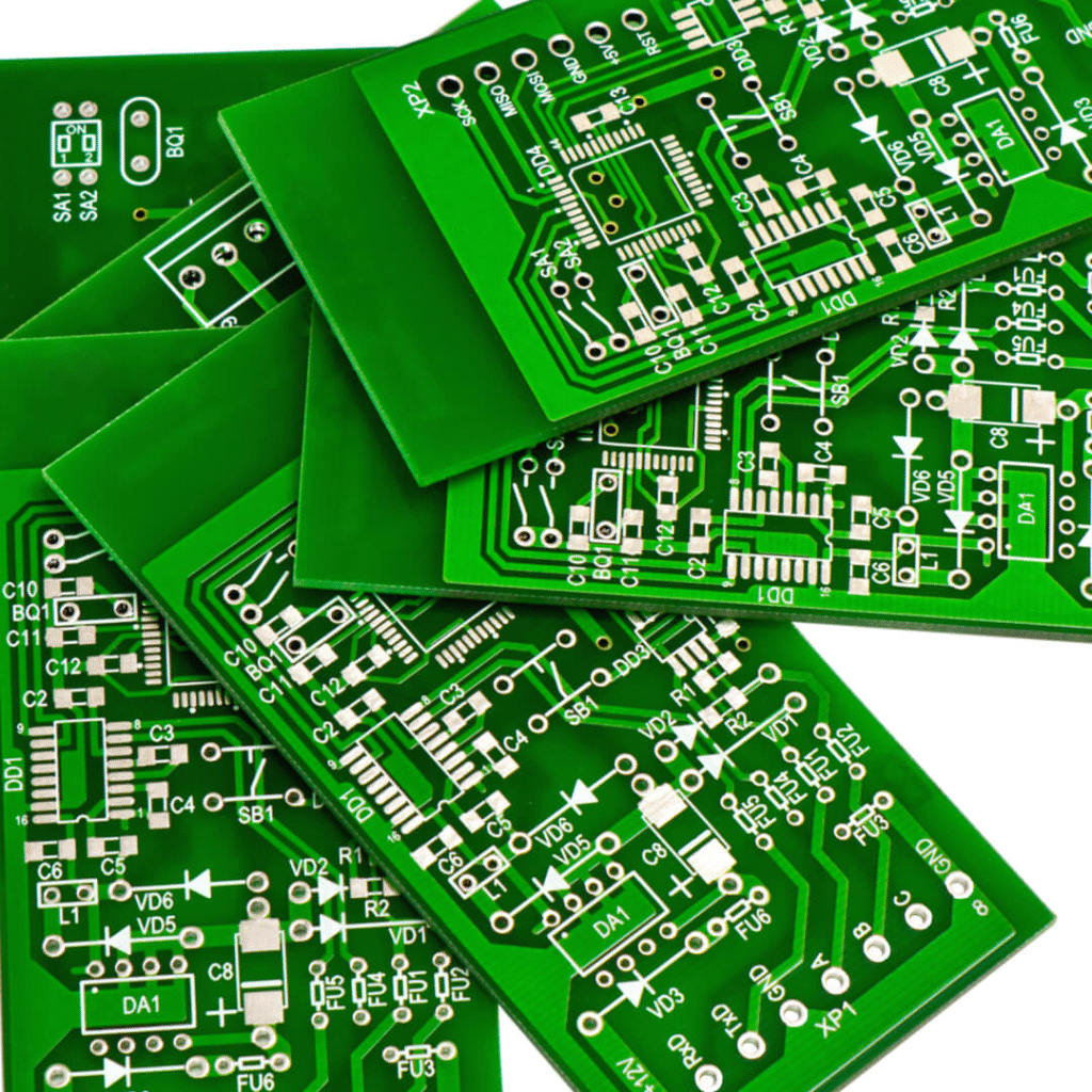
A PCB (Printed Circuit Board) is the “blank slate” of electronics. Think of it as the skeleton that holds everything together—no muscles, no nerves, just structure.
It’s made up of three core parts:
- The insulating substrate (usually FR-4, the industry workhorse)
- Thin copper traces that map out where signals will flow
- Pads for soldering components and vias to connect layers
At this stage, it’s just a piece of plastic with copper patterns—useless on its own. No resistors, no ICs, no solder joints. It’s a blueprint for the circuit, but it tells you nothing about whether that blueprint can be built reliably. I’ve had clients send perfect PCBs to assembly, only to find the pad sizes are too small for high-speed placement, or the trace spacing causes short circuits once components are soldered. A PCB can check every spec box and still be a nightmare for PCBA.
What Is a PCBA?
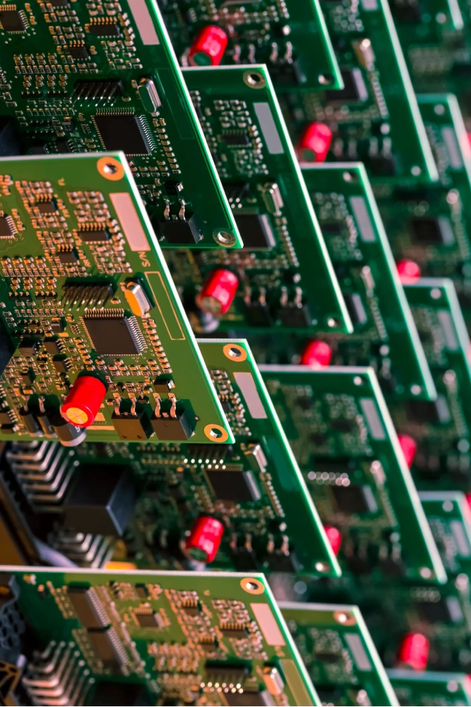
PCBA stands for Printed Circuit Board Assembly—this is where the blank slate comes to life. It’s the PCB after every component has been mounted, soldered, and tested.
Here’s what happens in this stage:
- SMT (Surface Mount Technology) or through-hole processes place resistors, capacitors, ICs, connectors, and other parts
- Solder paste is melted (reflow soldering) or applied manually (hand soldering for prototypes) to form secure joints
- The board goes through inspection (AOI, X-ray) to catch defects like cold joints or misaligned components
This is where the complexity—and the risk—skyrockets. Most of the issues I’ve debugged in manufacturing (80% easy) happen here: solder bridges between pins, components popped off during reflow, thermal damage to sensitive ICs. A PCB is just metal and plastic; a PCBA is a functional electronic device. One is a part, the other is a product.
PCB vs PCBA: The Gap That Actually Matters
On paper, the difference is simple. In the factory, it’s night and day. Let’s cut through the jargon with a quick comparison:
| Aspect | PCB | PCBA |
| Stage | Bare board (pre-assembly) | Assembled, functional device |
| Function | None—just a layout | Full electrical functionality |
| Process Focus | Etching, drilling, plating | Placement, soldering, inspection |
| Risk Level | Low (mostly material/design specs) | High (process-dependent, variable) |
The key point? A perfect PCB doesn’t guarantee a perfect PCBA. I once worked on a project where the PCB passed all DFM (Design for Manufacturing) checks, but the component footprints were slightly off—nothing noticeable on the bare board, but when the pick-and-place machine ran at full speed, 15% of the ICs were misaligned. That’s the gap: PCB is about design, PCBA is about execution.
Why This Difference Breaks Manufacturing Projects
Most teams underestimate how much variability assembly adds. When you move from a prototype (small batches, slow placement, forgiving timelines) to volume production (thousands of boards per run, high-speed machines, tight thermal windows), the PCB’s “hidden flaws” start popping up.
Here’s what manufacturers have to control during PCBA that never matters for PCB:
- Placement accuracy down to 0.1mm (critical for tiny 0402 components or BGA chips)
- Solder paste volume consistency (too little = cold joints; too much = bridges)
- Thermal stress during reflow (some components can’t handle temperatures over 260°C)
- Component supply variability (a slightly different capacitor package can throw off placement)
I’ve seen a design that worked flawlessly in prototypes fail during ramp-up because the PCB’s trace width was too narrow—when the assembly line ran at full speed, the solder wicking caused open circuits. The PCB was “correct,” but the PCBA process exposed its weakness.
Why Everyone Mixes Them Up (I’ve Been Guilty Too)
Confusion starts in the prototype phase. When you’re building 5-10 boards, you hand-solder components, take your time, and tweak as you go. The PCB works, the PCBA works, so you assume the two are interchangeable.
But volume production is a different beast. The pick-and-place machine doesn’t “tweak”—it repeats the same motion 10,000 times. The reflow oven doesn’t “go easy” on sensitive components—it hits exact temperatures for exact times. What worked for 10 boards falls apart at 10,000 because the assembly process amplifies every tiny flaw in the PCB.
I once had a client insist, “The PCB is perfect—why is the PCBA yield so low?” We ran X-rays and found the vias were slightly undersized—no problem for hand-soldering, but a disaster for automated through-hole assembly. Prototype success lulls you into a false sense of security.
What This Means for Your Project
Treating PCB and PCBA as the same thing is like assuming a pile of lumber will build itself into a house. You’ll end up with:
- Unexpected rework (I’ve seen teams spend 2x the budget fixing solder defects)
- Low yields during ramp-up (10% good boards instead of 95%—kill your timeline)
- Delays from process tuning (figuring out why components keep falling off mid-production)
The fix? Involve your PCBA manufacturer early—before you finalize the PCB design. They’ll catch things like pad size, trace spacing, or component package compatibility that a PCB designer might miss. I always tell clients: a PCB is only as good as its ability to be assembled into a PCBA.
Takeaway
Here’s the bottom line, from someone who’s fixed too many manufacturing messes:
- A PCB defines the circuit layout—what goes where.
- A PCBA defines whether that layout can be built consistently, reliably, and at scale.
The difference isn’t just words—it’s where production risk lives. Miss that, and you’ll be fixing expensive problems when it’s too late to change the PCB. Get it right, and you’ll sail through prototype to volume production without breaking a sweat.
At the end of the day, electronics manufacturing is about execution—not just design. And execution starts with knowing the difference between a blank slate and a finished product.