
Choosing the right PCB surface finish is not only a PCB fabrication decision. It can directly affect solderability, SMT placement stability, storage life, inspection results, rework risk, and long-term PCBA reliability.
For many buyers, PCB surface finish may look like a small item in the Gerber file or quotation sheet. However, during actual PCB assembly, the wrong finish can lead to poor solder wetting, unstable solder joints, oxidation before assembly, higher rework costs, or unexpected production delays.
HASL, ENIG, and OSP are three common PCB surface finish options used in electronic products. Each finish has its own advantages, limitations, and suitable applications.
The best choice depends on several factors:
- Component package type
- SMT assembly complexity
- PCB storage time before assembly
- Product reliability requirements
- Cost target
- Inspection and testing requirements
This guide explains how different PCB surface finishes affect PCB assembly and how buyers can choose the right option before production.
Quick Answer
There is no single best PCB surface finish for every project.
HASL is often suitable for standard and cost-sensitive PCB assembly with larger components.
ENIG is often preferred for fine-pitch components, BGA, QFN, high-density PCB assembly, and longer storage requirements.
OSP can be a good option for cost-sensitive SMT production when storage time, handling, and production schedule are well controlled.
Key Takeaways
- PCB surface finish protects exposed copper pads from oxidation.
- It affects solderability, pad flatness, SMT stability, shelf life, and rework risk.
- HASL is cost-effective but has limited surface flatness.
- ENIG offers excellent flatness and better storage stability but costs more.
- OSP is flat and low-cost, but it is more sensitive to storage and handling.
- The right finish should be selected based on both PCB design and assembly process, not cost alone.
What Is PCB Surface Finish?
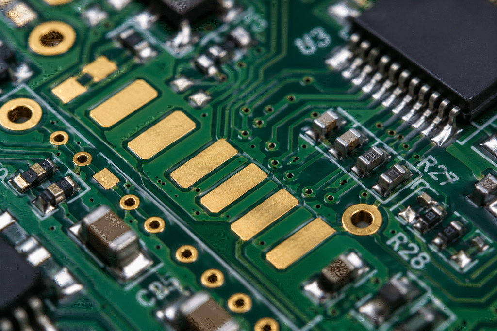
PCB surface finish is the final coating applied to the exposed copper pads on a printed circuit board.
Its main purpose is to:
- Protect copper pads from oxidation
- Provide a solderable surface for components
- Support stable solder joint formation during assembly
- Maintain pad condition before SMT or manual soldering
Without a proper PCB surface finish, bare copper can oxidize quickly. Once oxidation occurs, solder may not wet the pad properly during SMT assembly or manual soldering.
This can result in:
- Weak solder joints
- Poor electrical connection
- Unstable product performance
- Higher inspection and rework costs
Different PCB surface finish types perform differently in cost, flatness, shelf life, solderability, and process stability. That is why surface finish should be reviewed together with the BOM, Gerber files, component package types, and final product application.
Why PCB Surface Finish Matters in PCB Assembly
In real PCB assembly projects, surface finish problems often appear during soldering, inspection, or rework rather than during PCB fabrication itself.
A PCB may look acceptable before assembly, but problems can become visible once components are mounted and soldered.
1. Solderability and Wetting Quality
Solderability is one of the most important factors affected by PCB surface finish.
During reflow soldering, solder paste printing and pad surface condition must work together to form a strong and stable solder joint.
If the surface finish is oxidized, contaminated, too thin, uneven, or poorly controlled, solder may not spread properly.
Common results include:
- Poor solder wetting
- Cold solder joints
- Insufficient solder
- Weak solder joints
- Intermittent electrical connection
For simple PCB designs, these problems may be easier to detect and repair. For dense PCBA designs with fine-pitch ICs, BGA, QFN, or small passive components, solderability problems can be harder to identify and more expensive to fix.
2. SMT Placement Stability
Surface flatness is also important for SMT assembly.
Modern electronic products often use smaller components and denser layouts. Fine-pitch ICs, QFN packages, BGA components, and small passive components all require consistent pad flatness.
If the PCB surface is uneven, component placement may become less stable. This can affect:
- Solder paste contact
- Component alignment
- Reflow consistency
- Final solder joint quality
ENIG and OSP generally provide better surface flatness than HASL. This is one reason they are often used for high-density PCB assembly or designs with fine-pitch components.
3. Shelf Life Before Assembly
PCB surface finish also affects how long a PCB can be stored before assembly.
Some finishes have better oxidation resistance and longer shelf life, while others are more sensitive to handling, moisture, and storage conditions.
If PCBs are fabricated and assembled immediately, shelf life may not be a major concern.
But if boards need to be:
- Stored before assembly
- Shipped internationally
- Assembled in later batches
- Used for repeat production
then the PCB surface finish should be selected more carefully.
OSP, for example, can be suitable for cost-sensitive SMT production, but it is more sensitive to storage time and handling. ENIG usually offers better storage stability, which can be useful when production schedules are uncertain.
4. Rework and Inspection Risk
PCB surface finish can also influence AOI inspection, X-ray inspection, manual inspection, and rework.
For high-density PCB assembly, stable solder joint formation is important for inspection accuracy.
If the surface finish causes inconsistent solder wetting or poor pad condition, the risk of false defects, hidden defects, and rework increases.
Rework can also expose the PCB to additional heat. Some surface finishes handle multiple thermal cycles better than others.
When a product may require double-sided SMT, selective soldering, hand soldering, or rework, the finish should be evaluated as part of the complete assembly process.
Common PCB Surface Finish Types
There are several PCB surface finish options used in electronics manufacturing.
Common options include:
- HASL
- Lead-free HASL
- ENIG
- OSP
- Immersion silver
- Immersion tin
This article focuses on HASL, ENIG, and OSP because these three options are widely used in standard electronic products, cost-sensitive PCB assembly, and high-density SMT projects.
Each option can be suitable in the right situation.
The key is not to choose the most expensive finish automatically. The right choice should match the product design, assembly process, storage conditions, and reliability requirements.
HASL PCB Surface Finish
What Is HASL?
HASL stands for Hot Air Solder Leveling.
In this process, the PCB is coated with molten solder and then leveled by hot air knives. The result is a solder-coated surface over the exposed copper pads.
Traditional HASL used tin-lead solder. Lead-free HASL uses lead-free solder to meet modern environmental and compliance requirements. For products sold into regulated markets, buyers may also need to consider RoHS requirements for electrical and electronic equipment.
Advantages of HASL
HASL is a mature and widely used PCB surface finish. It is often selected for standard PCB assembly because of its practical cost and good solderability.
Main advantages include:
- Lower cost compared with ENIG
- Mature and widely available process
- Good solderability for many standard components
- Suitable for general electronic products
- Practical for larger pads and less dense PCB layouts
For many simple or standard PCB assemblies, HASL can still be a reliable and cost-effective option.
Limitations of HASL
The main limitation of HASL is surface flatness.
Because solder is applied and leveled across the pads, the final surface may not be perfectly even. This is usually acceptable for larger components, but it may create challenges for fine-pitch packages.
HASL may not be ideal for:
- Fine-pitch ICs
- BGA packages
- QFN components
- High-density PCB assembly
- Very small SMT components
- Designs requiring excellent pad flatness
Another factor is thermal exposure during the HASL process. The PCB is exposed to high temperature, which may not be suitable for every board structure or material.
When to Use HASL
HASL can be a good choice when the product uses standard components, larger pads, and a cost-sensitive design.
HASL may be appropriate for:
- Standard PCBA projects
- Cost-sensitive products
- Larger component packages
- Simple or medium-density PCB designs
- Products without BGA or very fine-pitch components
If the PCB design includes dense SMT components, very fine pitch, or high reliability requirements, ENIG or OSP may be more suitable.
ENIG PCB Surface Finish
What Is ENIG?
ENIG stands for Electroless Nickel Immersion Gold.
It consists of a nickel layer over the copper pad and a thin gold layer on top. The nickel layer acts as a barrier and solderable surface, while the gold layer helps protect the nickel from oxidation before assembly.
ENIG is commonly used when surface flatness, oxidation resistance, and longer storage life are important.
Advantages of ENIG
ENIG is often selected for high-density PCB assembly because it provides a flat and stable surface.
Main advantages include:
- Excellent surface flatness
- Good oxidation resistance
- Longer shelf life than OSP
- Suitable for fine-pitch ICs
- Suitable for BGA and QFN packages
- Good option for high-density PCB assembly
- Stable surface for demanding soldering requirements
Because of its flat surface, ENIG supports more consistent solder joint formation during SMT assembly.
This can be especially important for products with small components, dense layouts, or higher reliability expectations.
Limitations of ENIG
The main disadvantage of ENIG is cost.
It is usually more expensive than HASL and OSP. For very cost-sensitive products, this may affect the total PCB cost.
ENIG also requires good process control during PCB fabrication. Industry specifications such as IPC-4552B define requirements for Electroless Nickel / Immersion Gold deposit thickness and related performance criteria.
If the process is poorly controlled, reliability issues such as black pad may occur.
Although this is not common with qualified PCB suppliers, it is still a risk that buyers and engineers should understand.
When to Use ENIG
ENIG is often preferred when the PCB design requires better flatness, longer storage time, or higher assembly reliability.
ENIG may be suitable for:
- Fine-pitch ICs
- BGA components
- QFN packages
- High-density PCB assembly
- Products requiring longer PCB storage
- Industrial electronics
- Automotive electronics
- Medical or higher-reliability electronic products
ENIG is not always necessary for every project, but it can reduce assembly risk when component density and reliability requirements are higher.
OSP PCB Surface Finish
What Is OSP?
OSP stands for Organic Solderability Preservative.
It is an organic coating applied to exposed copper pads to protect them from oxidation before soldering.
Unlike HASL or ENIG, OSP does not add a metal coating layer. It creates a thin protective film that preserves solderability until assembly.
Advantages of OSP
OSP is commonly used in high-volume SMT production because it is cost-effective and provides a flat surface.
Main advantages include:
- Low cost
- Very flat pad surface
- Suitable for SMT assembly
- Environmentally friendly
- Good option for cost-sensitive products
- Suitable for high-volume production with controlled schedules
Because OSP provides a flat surface, it can support fine-pitch SMT assembly when the production process is well controlled.
Limitations of OSP
The main limitation of OSP is storage sensitivity.
OSP has a shorter shelf life than ENIG and can be affected by handling, moisture, contamination, and repeated thermal cycles.
OSP may not be ideal when:
- PCB storage time is long or uncertain
- Boards may be handled many times before assembly
- Multiple reflow cycles are required
- Rework is expected
- Production scheduling is not well controlled
If the PCB will be fabricated, shipped, stored, and assembled after a long delay, OSP may increase solderability risk.
When to Use OSP
OSP can be a practical choice for high-volume SMT projects when the production schedule is clear and well controlled.
OSP may be suitable for:
- Cost-sensitive electronic products
- High-volume SMT production
- Short storage time before assembly
- Flat pad requirements
- Products with controlled production and handling conditions
OSP is not a poor finish, but it needs proper storage and process control. When used correctly, it can balance cost and assembly performance.
HASL vs ENIG vs OSP: PCB Surface Finish Comparison
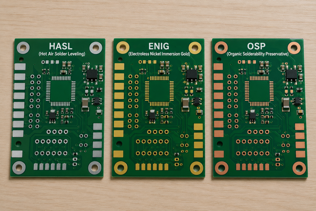
The table below compares HASL, ENIG, and OSP from a PCB assembly perspective.
| Factor | HASL | ENIG | OSP |
|---|---|---|---|
| Cost | Low | High | Low |
| Surface Flatness | Medium | Excellent | Good |
| Shelf Life | Good | Very Good | Shorter |
| Solderability | Good | Good | Good when well controlled |
| Fine-Pitch Suitability | Limited | Excellent | Good |
| BGA / QFN Suitability | Not ideal | Good | Depends on process control |
| Multiple Reflow Cycles | Good | Good | Limited |
| Storage Sensitivity | Medium | Low | High |
| Best For | Standard PCBA | High-density PCBA | Cost-sensitive SMT |
This comparison shows why there is no single best PCB surface finish for every project.
For simple and cost-sensitive PCB assembly, HASL may be enough.
For high-density designs with fine-pitch components, ENIG is often safer.
For high-volume SMT production with controlled storage and handling, OSP can be a good cost-effective option.
How to Choose the Right PCB Surface Finish for Your Project
The right PCB surface finish should be selected based on the complete product and assembly requirements, not only the PCB fabrication cost.
Check the Component Package Type
Component package type is one of the first things to review.
If the PCB uses larger components and standard pad sizes, HASL may be suitable.
If the design includes fine-pitch ICs, BGA, QFN, or very small passive components, surface flatness becomes more important. In this case, ENIG is often preferred.
OSP may also be considered if the production process is well controlled.
Consider the Storage Time Before PCB Assembly
Storage time can strongly affect solderability.
If the PCBs will be assembled soon after fabrication, OSP may be practical. If the boards may be stored for a longer time, ENIG can offer better protection against oxidation.
Buyers should confirm the production schedule before choosing a finish.
A low-cost surface finish may become expensive later if poor storage conditions lead to soldering defects or rework.
Review the Assembly Process
The PCB assembly process also matters.
A PCB that only goes through one standard SMT process has different requirements from a board that needs double-sided SMT, selective soldering, manual soldering, or rework.
Multiple thermal cycles can increase the risk for some finishes.
If the product has complex assembly steps, the surface finish should be reviewed together with the SMT process, inspection plan, and rework expectations.
Balance Cost and Reliability
Cost is always important, but surface finish should not be selected only by price.
A lower-cost finish may be reasonable for simple consumer electronics, but it may not be the right choice for high-reliability products.
For automotive electronics, industrial control products, medical devices, or products used in harsh environments, the cost of failure can be much higher than the cost difference between surface finish options.
A practical decision should balance:
- PCB cost
- Assembly stability
- Inspection requirements
- Storage risk
- Rework cost
- Long-term reliability
For buyers comparing quotations, this is also an important part of understanding the full PCBA cost breakdown.
Confirm Inspection and Testing Requirements
If the product requires AOI, X-ray inspection, functional testing, or final product assembly, the surface finish should support stable soldering results.
For example, BGA solder joints cannot be visually inspected in the same way as standard components. A stable surface finish and controlled assembly process are important for reducing hidden soldering risks.
Before production, buyers should confirm not only the PCB finish but also the inspection and testing plan.
Common Problems Caused by the Wrong PCB Surface Finish
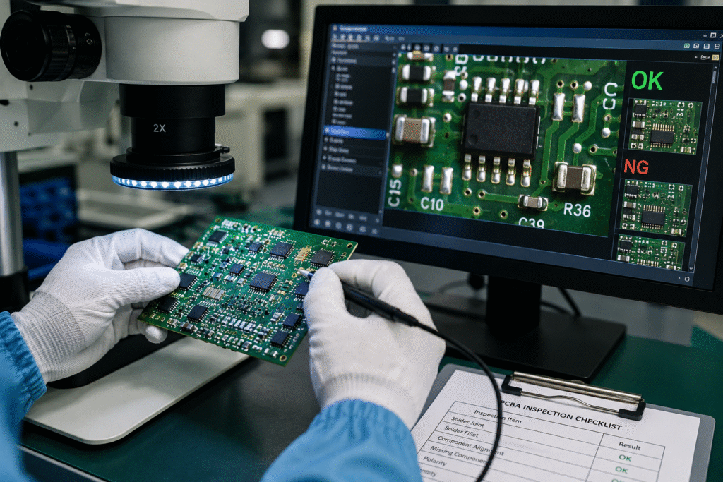
Choosing the wrong PCB surface finish does not always cause immediate failure.
In many cases, the problem appears during assembly, inspection, testing, or later product use.
Poor Solder Wetting
Poor solder wetting occurs when solder does not spread properly across the pad surface.
This can be caused by oxidation, contamination, poor storage, or an unsuitable surface finish.
Poor wetting may lead to weak solder joints, unstable electrical connection, or soldering defects during reflow.
Insufficient or Weak Solder Joints
If the surface finish does not support stable solder formation, solder joints may become insufficient, uneven, or mechanically weak.
This is especially risky for connectors, power components, fine-pitch ICs, and components exposed to vibration or repeated use.
Component Alignment Issues
Uneven surface finish can affect how components sit on the solder paste before and during reflow.
For small components or fine-pitch packages, this can increase the risk of:
- Misalignment
- Tombstoning
- Inconsistent solder joints
- Reflow defects
HASL may create more flatness challenges than ENIG or OSP, especially for dense SMT layouts.
Oxidation Before Assembly
If PCBs are stored too long or handled improperly, oxidation can reduce solderability.
This risk is higher for finishes with shorter shelf life or higher storage sensitivity.
Good packaging, controlled storage, and clear assembly scheduling are important, especially when using OSP.
Higher Rework Cost
Surface finish problems can increase rework time and cost.
Rework may require extra labor, additional inspection, and repeated heat exposure. In high-density PCBA, rework can also increase the risk of damaging nearby components or pads.
A suitable PCB surface finish can help reduce these risks before mass production begins.
What Buyers Should Confirm Before PCB Production
Before confirming PCB fabrication and assembly, buyers should review several key points with the supplier.
Use this checklist before production:
- What PCB surface finish is specified in the Gerber file?
- Are there BGA, QFN, or fine-pitch components?
- How long will the PCB be stored before assembly?
- Will the board go through single-sided or double-sided SMT?
- Are multiple reflow cycles required?
- Is the product cost-sensitive or reliability-sensitive?
- Are RoHS or other compliance requirements needed?
- Will AOI, X-ray, or functional testing be required?
- Does the final product require plastic enclosure assembly or box build integration?
This information helps the supplier evaluate whether HASL, ENIG, or OSP is more suitable for the project.
For buyers preparing project files, a complete PCB Assembly RFQ Checklist can also help reduce communication gaps before quotation and production.
How Cindy Mould Supports PCB Surface Finish Review
At Cindy Mould, PCB surface finish is reviewed as part of the complete electronics manufacturing process.
Instead of looking at the PCB finish as a separate fabrication detail, we evaluate it together with the BOM, Gerber files, component package types, assembly process, and product application.
Gerber and BOM Review
Before PCB assembly, our team reviews the Gerber files and BOM to understand pad design, component package types, assembly density, and possible production risks.
If the design includes fine-pitch components, BGA, QFN, or special soldering requirements, the surface finish selection should be checked carefully before production.
PCB Assembly Process Evaluation
Surface finish affects more than the PCB itself.
It also influences:
- Solder paste printing
- SMT placement
- Reflow soldering
- AOI inspection
- X-ray inspection
- Manual inspection
- Possible rework
By reviewing the complete assembly process, we help customers reduce avoidable soldering risks and improve PCBA production stability.
Prototype and Small-Batch Production Support
Prototype and small-batch production are useful stages for identifying potential assembly risks before mass production.
If a surface finish causes soldering inconsistency, inspection difficulty, or handling sensitivity, these issues should be found early.
This is especially important for custom electronic products where the PCB, enclosure, wiring, testing, and final assembly need to work together.
Complete Electronics Manufacturing Support
Cindy Mould provides support for PCB Services, functional testing, plastic enclosure manufacturing, product assembly, and complete electronic product integration.
For projects that include both PCBA and mechanical enclosure assembly, reviewing PCB surface finish early can help reduce production risks later in the process.
Conclusion
PCB surface finish affects much more than PCB fabrication cost.
It can influence:
- Solderability
- SMT assembly stability
- Storage life
- Inspection quality
- Rework risk
- Long-term PCBA reliability
HASL, ENIG, and OSP each have their own suitable applications.
HASL can be practical for standard and cost-sensitive PCB assembly. ENIG is often preferred for fine-pitch, BGA, QFN, and high-density PCB designs. OSP can be a good option for high-volume SMT production when storage time and handling are well controlled.
The best choice depends on the product design, component package type, assembly process, storage schedule, reliability requirements, and cost target.
If you are not sure which PCB surface finish is suitable for your project, Cindy Mould can review your Gerber files, BOM, component layout, and assembly requirements before production.
FAQ
What is the best PCB surface finish for SMT assembly?
There is no single best PCB surface finish for every SMT assembly project.
ENIG is often preferred for fine-pitch and high-density PCB assembly, while HASL and OSP can be suitable for standard or cost-sensitive products.
Is ENIG better than HASL?
ENIG provides better surface flatness and longer shelf life, but it is more expensive.
HASL is still suitable for many standard PCB assembly projects with larger components and less dense layouts.
Is OSP suitable for PCB assembly?
Yes. OSP can be suitable for PCB assembly when storage time, handling, and production schedule are well controlled.
It is often used in cost-sensitive and high-volume SMT production.
Which PCB surface finish is best for BGA components?
ENIG is commonly preferred for BGA components because it provides a flat surface and good solderability.
For BGA designs, surface finish should be reviewed together with the PCB layout, solder paste process, and inspection plan.
Does PCB surface finish affect PCBA cost?
Yes. PCB surface finish affects not only PCB fabrication cost but also assembly stability, storage risk, inspection requirements, and possible rework cost.
A lower-cost finish may not always reduce the total project cost if it increases production risk.