Introduction: When Production Looks Fine but Products Still Fail
PCB assembly defects are a persistent challenge in electronics manufacturing, particularly in projects that move from prototype validation into mass production.
In many cases, products pass inspection, meet test requirements, and appear stable during initial builds. However, once production scales or products enter real-world environments, failures begin to emerge. These failures are often inconsistent, difficult to reproduce, and costly to resolve.
For procurement teams and engineering managers, this creates a recurring problem:
production data suggests acceptable quality, yet customer feedback indicates otherwise.
The root cause is rarely a single defect. Instead, PCB assembly defects typically result from a combination of process variation, incomplete inspection coverage, and misalignment between design and manufacturing conditions.
This article provides a structured approach to understanding PCB assembly defects—not just as isolated issues, but as part of a broader manufacturing system that must be controlled, measured, and continuously improved.
Why PCB Assembly Defects Increase During Mass Production
A common misconception is that if a product works during prototype builds, it will perform the same in mass production. In reality, scaling production introduces new variables that can significantly affect assembly quality.
Variation Amplification at Scale
During prototype builds, processes are often closely monitored, and adjustments can be made quickly. In mass production, however, even small variations—such as slight changes in solder paste viscosity or temperature fluctuations—can become amplified across thousands of units.
These variations may not cause immediate defects but can lead to inconsistent solder joints and long-term reliability issues.
Handoff Gaps Between Process Stages
PCB assembly involves multiple stages, including solder paste printing, component placement, reflow soldering, inspection, and final assembly integration.
When these stages are not tightly coordinated, defects can be introduced or missed. For example, insufficient solder paste may not be detected early and only becomes apparent during functional testing or field use.
Inspection Limitations
Inspection systems such as AOI and functional testing are essential but have limitations. They are primarily designed to detect visible or functional defects, not to ensure that underlying process conditions are stable.
As a result, products may pass inspection while still containing latent defects that lead to failure later.
Common PCB Assembly Defects: Indicators of System Instability
PCB assembly defects are often treated as isolated technical problems. In practice, they are indicators of instability within the manufacturing system.
Cold Solder Joints
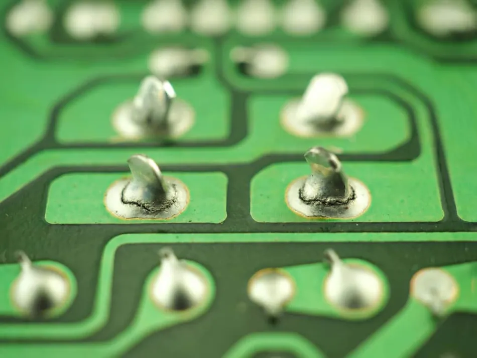
Example of a cold solder joint showing poor wetting between the component lead and PCB pad.
Cold solder joints result from incomplete solder wetting and bonding. This is often related to improper thermal control during soldering. To better understand how temperature profiles affect solder joint quality, see our guide on reflow soldering profile optimization.
System implication
Indicates unstable thermal profiles or poor material control.
Operational risk
High likelihood of intermittent failures, especially under thermal or mechanical stress.
Solder Bridging
Solder bridging creates unintended electrical connections between adjacent pads.
System implication
Reflects poor control of solder paste deposition and placement accuracy.
Operational risk
Immediate functional failure and potential component damage.
Tombstoning
Tombstoning occurs when one side of a component lifts during reflow.
System implication
Indicates imbalance in thermal distribution or solder paste volume.
Operational risk
Open circuits and reduced assembly efficiency.
Insufficient Solder
Insufficient solder leads to weak or unreliable joints.
System implication
Highlights inconsistency in solder paste printing or stencil condition.
Operational risk
Latent failures that may appear during field use.
Voiding
Voids are air pockets within solder joints, particularly in BGA components.
System implication
Indicates issues in reflow profile or material handling.
Operational risk
Reduced thermal performance and long-term reliability concerns.
Component Misalignment
Misalignment occurs when components are not correctly positioned on pads.
System implication
Points to equipment calibration issues or PCB stability problems.
Operational risk
Functional defects and aesthetic quality issues.
Hidden Root Causes Behind PCB Assembly Defects
Understanding defects requires looking beyond visible symptoms to underlying causes.
Process Variability
Variability in key parameters—such as solder paste thickness, placement accuracy, and temperature profiles—can accumulate and create inconsistent results.
Incomplete Process Control
Without clear control limits and monitoring systems, processes may drift over time, increasing defect rates.
Design Constraints
Certain PCB designs are inherently more sensitive to assembly conditions. Tight spacing, thermal imbalance, and complex layouts increase the likelihood of defects.
Industry guidelines from IPC (such as IPC-A-610 for acceptability and IPC-2221 for design guidelines) provide frameworks for aligning design with manufacturing capabilities, but these must be integrated into early project stages.
A Structured Framework for Controlling PCB Assembly Defects
Reducing PCB assembly defects requires a system-level approach rather than isolated fixes.
1. Solder Paste Control
Solder paste is a primary driver of assembly quality.
Key actions include:
- Controlling storage temperature and humidity
- Monitoring paste viscosity and shelf life
- Standardizing printing parameters
- Optimizing stencil design
SPI systems should be used to verify solder volume before placement.
2. Reflow Process Stability
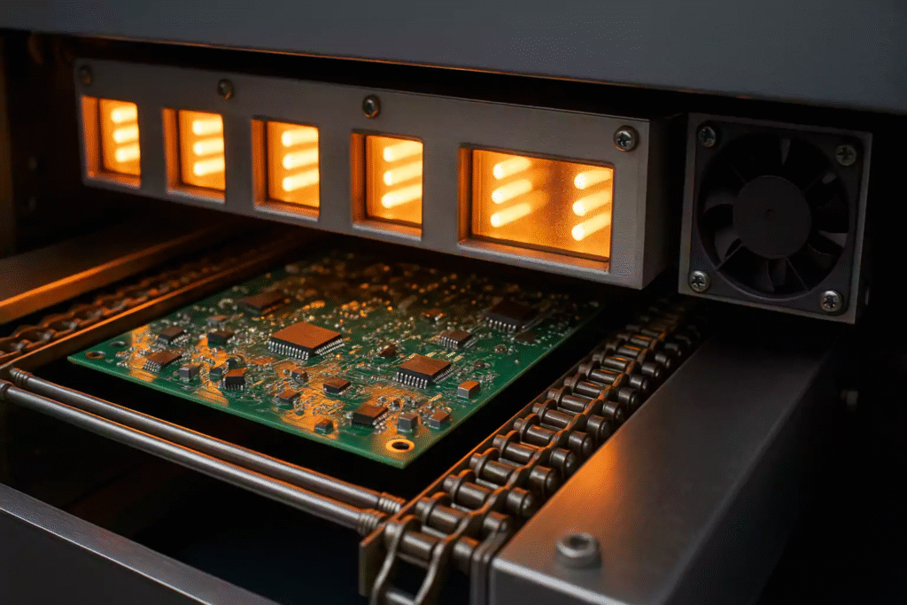
The reflow process determines the final quality of solder joints. For a broader understanding of how reflow fits into the overall PCB assembly workflow, refer to this PCB assembly process guide.
Control points include:
- Heating rate and soak time
- Peak temperature consistency
- Cooling profile
Stable reflow conditions reduce defects such as cold joints, tombstoning, and voiding.
3. Layered Inspection Strategy
An effective inspection system combines multiple methods. To understand how each inspection method works and when to use them, see our comparison of AOI vs AXI vs SPI in PCB inspection:
- SPI for early-stage control
- AOI for visual defects
- AXI for hidden joints
- ICT and functional testing for electrical validation
This layered approach improves defect detection and containment.
4. DFM Integration
Design for Manufacturing (DFM) ensures that PCB designs are compatible with assembly processes.
Key considerations include:
- Pad geometry and spacing
- Thermal balance
- Component placement
Early DFM reviews reduce production risks.
5. Final Assembly Alignment
PCB assembly must be aligned with final product assembly. For a deeper understanding of how integration impacts product reliability, see our guide on PCB assembly vs box build differences. Mechanical stress, cable routing, and enclosure constraints can all impact solder joint reliability.
A fully integrated manufacturing approach ensures that these factors are considered together.
Practical Workflow: From Defect Detection to Process Control
A structured workflow helps transform defect management into process control.
- Identify defect patterns through inspection and testing
- Trace defects back to process parameters and root causes
- Implement corrective actions in printing, placement, or reflow
- Validate improvements through controlled pilot runs
- Standardize processes and monitor performance metrics
This approach ensures continuous improvement rather than repeated troubleshooting.
Key Metrics for Managing PCB Assembly Quality
To effectively control PCB assembly defects, organizations should track key performance indicators.
| KPI | Definition | Target Range |
|---|---|---|
| First Pass Yield (FPY) | Units passing without rework | 98–99.5% |
| Defect Rate (PPM) | Defects per million units | <1000 PPM |
| Rework Rate | Percentage of units reworked | <2–5% |
| Field Failure Rate | Failures after shipment | <1% |
Monitoring these metrics provides visibility into process stability and helps guide improvement efforts.
Case Insight: Why Integration Reduces Defect Risk
In projects where PCB assembly, enclosure manufacturing, and final assembly are managed by separate suppliers, communication gaps can increase defect risk.
For example, a minor design change in the enclosure may affect connector alignment, which in turn introduces mechanical stress on solder joints. If these changes are not coordinated, defects may appear during final assembly or field use.
An integrated manufacturing approach improves coordination, reduces handoff delays, and ensures that design changes are consistently applied across all stages.
Conclusion: Moving from Defect Fixing to System Control
PCB assembly defects are not simply technical issues—they are indicators of how well a manufacturing system is controlled.
While individual defects can be identified and corrected, long-term improvement requires a shift toward process stability, design alignment, and integrated manufacturing.
By implementing a structured control framework and monitoring key performance metrics, manufacturers can achieve:
- Higher production yield
- Lower rework and defect rates
- Improved product reliability
- More predictable delivery performance
Ultimately, the goal is not just to fix defects, but to build a manufacturing system where defects are minimized by design.
Call to Action
If your project is experiencing recurring PCB assembly defects or inconsistent production quality, it may be time to evaluate your manufacturing approach from a system perspective.
At CINDY Mould, we provide integrated solutions covering PCB assembly and final product assembly, helping customers achieve stable processes, reliable quality, and efficient production.
Contact us to discuss your project and identify potential risks before they impact your production.