
A through-hole component may fit perfectly in the PCB design but become difficult to insert during assembly. A connector may align correctly in CAD but not sit flat on the manufactured board. In many cases, the problem is not the component—it is how the PCB hole size was defined.
Selecting the correct PCB finished hole size is essential for reliable component insertion, soldering, connector alignment, and mechanical assembly.
One of the most common sources of confusion is the difference between drill size and finished hole size.
The drill size refers to the hole created during the drilling process, while the finished hole size is the actual diameter after drilling, copper plating, surface treatment, and other manufacturing processes have been completed.
For plated holes, these two dimensions are usually not the same.
Understanding their relationship is essential when designing holes for through-hole components, connectors, press-fit pins, mounting screws, and mechanical locating features. This guide explains how drilling, plating, tolerances, and assembly requirements affect PCB finished hole size—and what information should be included in the manufacturing files.
What Is PCB Finished Hole Size?
PCB finished hole size is the final internal diameter of a hole after all relevant PCB manufacturing processes have been completed.
It is the dimension that ultimately determines whether a component lead, connector pin, locating post, or fastener will fit into the board.
For a plated through hole, the manufacturing process generally includes:
- Drilling the initial hole
- Cleaning and preparing the hole wall
- Depositing conductive copper
- Building up the required copper thickness through electroplating
- Applying the specified surface finish
- Inspecting the final hole size
Because copper is added to the wall of a plated hole, its final diameter becomes smaller than the initial drilled diameter.
This is why designers should clearly distinguish between the following terms:
| Term | Meaning |
|---|---|
| Drill size | The nominal diameter used during the drilling process |
| Finished hole size | The final hole diameter after plating and manufacturing |
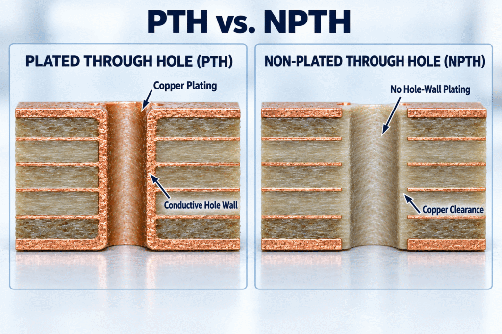
| PTH | Plated Through Hole with conductive material on the hole wall |
| NPTH | Non-Plated Through Hole without conductive hole-wall plating |
| Hole tolerance | The acceptable variation in the final hole diameter |
| Positional tolerance | The acceptable variation in the location of the hole center |
The finished hole size is usually the most important value for component insertion and mechanical assembly.
Drill Size vs. PCB Finished Hole Size
Although drill size and finished hole size are related, they describe two different stages of PCB manufacturing.
The drill creates the initial opening in the PCB material. If the hole is specified as a plated through hole, copper is then deposited and plated onto the inside wall. This plating reduces the available internal diameter.
A simplified relationship can be expressed as:
Finished hole diameter ≈ Drill diameter − Total plating build-up
If the plating thickness on each side of the hole wall is represented by t, the theoretical relationship is:
Finished hole diameter ≈ Drill diameter − 2t
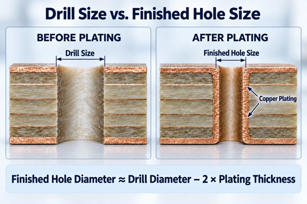
However, this formula is only useful for understanding the basic relationship. Actual production results can also be affected by:
- Drill diameter tolerance
- Drill wear
- Hole-wall preparation
- Copper plating distribution
- PCB thickness
- Hole aspect ratio
- Surface finish
- Manufacturing process capability
For this reason, the PCB manufacturer normally selects the appropriate production drill size based on the required finished hole size.
Designers should not assume that one fixed drill compensation value will work for every PCB supplier, board construction, or plating requirement.
A Simple Example
Suppose a through-hole component has a pin diameter of 0.80 mm.
The PCB hole should not normally be designed at exactly 0.80 mm because additional space may be needed for:
- Component pin dimensional variation
- PCB hole tolerance
- Pin position variation
- Automatic or manual insertion
- Solder flow around the pin
- Assembly alignment
After reviewing these factors, the designer may specify a finished hole size of 1.00 mm.
The PCB manufacturer then selects a larger production drill size to compensate for the copper that will be added to the hole wall. The exact drill size should be based on the manufacturer’s process and the specified plating requirement.
The key point is that 1.00 mm represents the required final opening—not necessarily the diameter of the drill used to create it.
How Plating Affects PCB Finished Hole Size
Copper plating inside a hole performs several important functions.
It creates electrical connections between PCB layers, supports soldering, and contributes to the reliability of vias and component holes. At the same time, it changes the physical diameter of the hole.
Copper Plating Inside the Hole
For a plated through hole, copper is deposited around the entire internal wall. As the plating becomes thicker, the opening becomes smaller.
The amount of plating build-up may depend on:
- Required hole-wall copper thickness
- PCB thickness
- Hole diameter
- Hole aspect ratio
- Copper distribution across the panel
- Plating process control
- Reliability requirements
- Applicable customer specifications
A standard through-hole component and a press-fit connector may therefore require different levels of dimensional control.
Plating Is Not Always Perfectly Uniform
The theoretical calculation assumes that copper is deposited evenly around the hole. In production, some variation is unavoidable.
Small holes, thick boards, high aspect ratios, and uneven copper distribution can make plating more difficult to control. This is one reason why the manufacturer needs an acceptable finished-hole tolerance rather than one absolute dimension with no variation.
Does Surface Finish Affect Hole Size?
Surface finishes such as HASL and ENIG are primarily applied to exposed conductive surfaces to improve solderability and protect the copper.
Depending on the finish and production process, they may have a secondary effect on the usable opening of a plated hole. However, surface finish should not be treated as a substitute for proper drill and plating calculations.
The final PCB finished hole size requirement should still be defined together with its allowed tolerance.
PTH and NPTH Have Different Requirements
Before selecting a hole size, it is necessary to determine whether the hole should be plated or non-plated.
Plated Through Holes
A plated through hole has conductive copper on the hole wall. Common applications include:
- Through-hole component leads
- Pin headers
- Connectors
- Test points
- Conductive vias
- Press-fit pins
- Grounding or chassis connections
The required PCB finished hole size must account for both the component lead dimensions and the copper added to the hole wall.
When designing a PTH, engineers should consider:
- Finished hole diameter
- Copper plating requirement
- Annular ring size
- Component lead dimensions
- Insertion clearance
- Solder filling
- Hole diameter tolerance
- Hole location tolerance
Because plating reduces the opening, the initial drill must normally be larger than the required finished hole.
Non-Plated Through Holes
An NPTH does not have conductive plating on the hole wall. It is commonly used for:
- Mounting screws
- Locating pins
- Plastic bosses
- Mechanical supports
- PCB alignment features
- Snap-fit structures
For NPTH features, the final hole size may be closer to the mechanical drill or routing size because there is no copper plating inside the hole. Manufacturing tolerances still apply, however, and the finished dimension must be suitable for the mating hardware.
Designers should also define sufficient clearance between an NPTH and surrounding copper features when electrical isolation is required.
PTH and NPTH features must be clearly separated in the drill data and fabrication documentation. If the hole type is unclear, the PCB supplier may need to stop the job and request clarification.
Understanding PCB Hole Tolerances
No machining or plating process produces exactly the same dimension on every hole. A hole tolerance defines the acceptable variation around the nominal finished size.
PCB finished hole size tolerance defines the acceptable variation in the final diameter after drilling and plating.
For example, a drawing may specify a nominal finished hole diameter together with a positive and negative tolerance. The PCB manufacturer must then keep the inspected holes within that range.
Variation can result from:
- Drill-bit manufacturing tolerance
- Drill wear during production
- Tool movement or runout
- PCB material behavior
- Hole-wall preparation
- Copper plating variation
- Board thickness
- Thermal and mechanical processing
Standard and Tight Tolerances
Many ordinary component holes can use the PCB supplier’s standard production tolerance.
Some applications require tighter control, including:
- Press-fit connectors
- High-pin-count through-hole connectors
- Precision locating holes
- Mechanical alignment features
- Holes that interact with enclosure components
- Controlled-fit fastener holes
A tighter tolerance is not automatically better. It may require additional process control, inspection, tool selection, or supplier review. This can increase manufacturing cost and lead time.
The tolerance should therefore be based on the actual function of the hole.
For broader industry guidance, designers can also refer to IPC standards and education resources covering PCB design, manufacturing, quality, and reliability.
Diameter Tolerance vs. Positional Tolerance
Hole diameter and hole position are different requirements.
Diameter tolerance controls how large or small the hole can be.
Positional tolerance controls how far the center of the manufactured hole can move from its intended location.
A connector hole may have the correct diameter but still create an assembly problem if several holes are slightly misaligned. Positional accuracy becomes especially important for:
- Multi-pin connectors
- Rigid component arrays
- Enclosure mounting points
- PCB-to-housing locating features
- Mating board assemblies
Both size and position should be reviewed when the PCB must interface with mechanical components.
How to Select the Right PCB Finished Hole Size
Selecting the correct finished hole size involves more than adding an arbitrary allowance to a component lead.
1. Confirm the Maximum Lead or Pin Size
Start with the component manufacturer’s datasheet.
Do not rely only on the nominal pin diameter. Check:
- Maximum pin width or diameter
- Pin dimensional tolerance
- Pin cross-sectional shape
- Lead coating or plating
- Pin straightness
- Position tolerance across multiple pins
A square or rectangular pin may require a different hole calculation from a round pin.
2. Add Appropriate Assembly Clearance
The clearance between the component lead and the finished hole should support the actual assembly process.
The required clearance may depend on:
- Manual or automatic insertion
- Number of pins
- Pin alignment
- Component body tolerance
- PCB hole tolerance
- Soldering method
- Required solder flow
- Product reliability requirements
Too little clearance can make insertion difficult and increase the risk of bent pins, damaged plating, poor seating, or assembly delays.
Too much clearance can also create problems. The component may move before soldering, alignment may become unstable, and solder filling may become more difficult to control.
The goal is a practical assembly window—not the smallest or largest possible hole.
3. Identify the Hole Function
Determine whether the feature is a:
- Plated component hole
- Non-plated mounting hole
- Via
- Press-fit hole
- Tooling hole
- Locating hole
- Plated slot
- Non-plated slot
Each type has different electrical, mechanical, and manufacturing requirements.
4. Define the Finished Size and Tolerance
The fabrication documentation should clearly identify the required finished hole size and acceptable tolerance.
Do not provide an unexplained drill diameter and expect the manufacturer to determine the intended final fit.
5. Confirm the PCB Manufacturer’s Capability
Before releasing the design, confirm:
- Minimum finished hole size
- Available hole-size tolerances
- Minimum annular ring
- Supported board thickness
- Allowable hole aspect ratio
- Hole-wall copper capability
- Press-fit hole capability
- Plated-slot capability
- Relevant inspection methods
Early confirmation is particularly important for thick boards, small holes, press-fit connectors, and mechanically critical features.
These requirements can also be reviewed as part of our PCB assembly services before fabrication and assembly begin.
PCB Finished Hole Size for Common Applications
Different applications require different design priorities.
| Application | Main Design Consideration |
|---|---|
| Through-hole components | Lead size, insertion clearance, solder flow and component seating |
| Multi-pin connectors | Hole diameter, accumulated pin-position error and connector alignment |
| Press-fit connectors | Tight hole tolerance, copper thickness, hole shape and supplier capability |
| Mounting holes | Screw size, washer clearance, enclosure alignment and mechanical tolerance |
| Locating holes | Positional accuracy and fit with pins, posts or fixtures |
| Vias | Electrical connection, plating reliability, annular ring and aspect ratio |
| Plated slots | Lead shape, slot width, slot length, plating and routing tolerance |
| Non-plated slots | Mechanical fit, tool radius and clearance from nearby copper |
There is no single finished hole allowance that is correct for every application. The part datasheet, assembly method, board construction, and supplier capability must be considered together.
Common PCB Hole Size Design Mistakes
Several avoidable mistakes can create delays during PCB fabrication or product assembly.
Many PCB finished hole size problems begin with unclear design assumptions or inconsistent manufacturing data.
1. Treating Drill Size as Finished Hole Size
If a plated hole is drilled at the same diameter as the required final opening, the plating process can make the hole too small.
2. Not Distinguishing PTH from NPTH
A mounting hole intended to be non-plated may be produced as a plated hole if the documentation is unclear. This can change both its electrical behavior and usable diameter.
3. Using Only the Nominal Pin Dimension
Component pins have manufacturing tolerances. Designing around only the nominal value may leave insufficient clearance for the largest acceptable pins.
4. Leaving Too Little Assembly Clearance
A hole may appear acceptable in CAD but become difficult to assemble once pin tolerance, hole tolerance, and positional variation are combined.
5. Applying Tight Tolerances to Every Hole
Unnecessarily tight tolerances can increase cost without improving product performance. Critical holes should be identified separately from ordinary component holes.
6. Ignoring Annular Ring Requirements
Increasing the finished hole size without reviewing the pad diameter can reduce the remaining annular ring and create a new manufacturing risk.
7. Providing Inconsistent Manufacturing Files
Conflicts between the fabrication drawing, drill table, NC drill data, Gerber files, and assembly documentation can delay engineering review and production.
What Should Be Included in PCB Manufacturing Files?
Clear documentation helps the PCB manufacturer understand the design intent and select the correct tooling and process compensation.
The PCB finished hole size and its tolerance should be clearly identified in the fabrication drawing or drill table.
Depending on the board, the manufacturing package should include:
- Required finished hole diameters
- Hole-size tolerances
- Clear PTH and NPTH identification
- Drill table or hole chart
- NC drill files
- Plated and non-plated slot dimensions
- Press-fit hole requirements
- Hole-wall copper requirements
- Board thickness
- Relevant fabrication notes
- Gerber or other approved PCB production data
- Mechanical drawings for critical interfaces
All dimensions and units should be consistent across the file package.
When a drill file contains nominal tool sizes, the fabrication notes should clarify whether they represent finished dimensions or production drill dimensions. Ambiguous terminology can lead to different interpretations.
Why DFM Review Should Happen Before Production
A design for manufacturability review can identify hole-related risks before PCB fabrication begins.
A DFM review helps confirm whether each PCB finished hole size is suitable for the component, plating process, and assembly method.
A structured quality and process control approach can further help identify dimensional, plating, and assembly risks before production.
A practical hole review may include:
- Comparing finished holes with component pin dimensions
- Checking PTH and NPTH definitions
- Reviewing annular ring dimensions
- Confirming drill-to-copper clearance
- Evaluating board thickness and hole aspect ratio
- Identifying unnecessary tight tolerances
- Reviewing connector and enclosure alignment
- Checking plated-slot requirements
- Confirming press-fit specifications
- Comparing fabrication data with assembly drawings
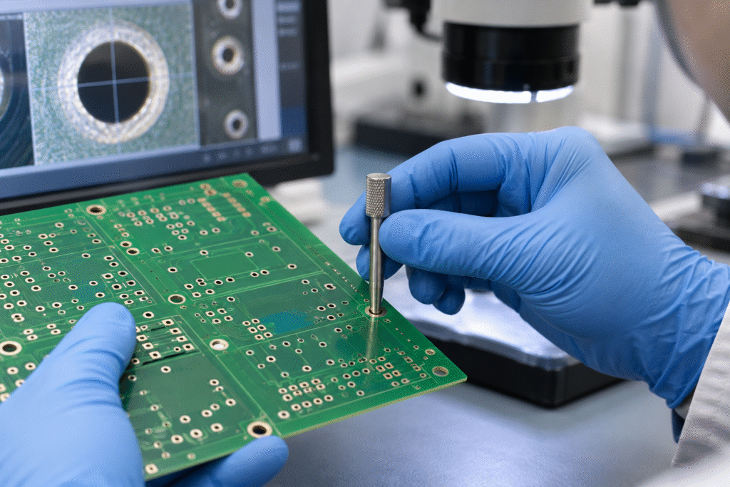
Finding these issues before production is usually faster and less expensive than correcting a board that has already been manufactured.
For projects that combine PCB assembly, plastic enclosures, wiring, and complete product assembly, hole dimensions should also be reviewed in the context of the complete product. A PCB mounting hole may be acceptable by itself but still create an alignment problem with an enclosure boss, display, connector opening, or external button.
Frequently Asked Questions
Is PCB finished hole size the same as drill size?
No. Drill size describes the initial drilled opening, while finished hole size describes the final diameter after the required manufacturing processes. For plated holes, the finished diameter is normally smaller because copper is added to the hole wall.
How much larger should the drill be than the finished hole?
There is no universal compensation value. The required difference depends on plating thickness, board construction, hole geometry, tolerance, and the PCB manufacturer’s process. The manufacturer should select the production drill based on the required finished hole.
Should a PCB drawing specify drill size or finished hole size?
For holes that affect component insertion or mechanical fit, the drawing should clearly state the required finished hole size and tolerance. If drill sizes are also included, their meaning must be defined to avoid ambiguity.
What is the difference between PTH and NPTH?
A PTH has conductive plating on its internal wall and can provide electrical connection between layers. An NPTH has no conductive hole-wall plating and is generally used for mechanical mounting, locating, or isolation purposes.
Why do press-fit holes require tighter control?
Press-fit performance depends on controlled interference between the connector pin and the plated hole. Hole diameter, hole shape, copper thickness, material behavior, and positional accuracy can all affect insertion force and connection reliability.
Does a tighter hole tolerance increase PCB cost?
It can. Tight tolerances may require more precise tooling, additional process control, more inspection, or special manufacturer approval. Tolerances should match the functional requirement rather than being tightened by default.
Can enlarging the hole solve an insertion problem?
Sometimes, but the pad diameter, annular ring, soldering process, and mechanical stability must also be reviewed. Enlarging the hole without checking these factors may introduce other manufacturing or reliability risks.
Conclusion
PCB finished hole size is a small design detail with a direct effect on fabrication, component insertion, soldering, connector alignment, and final product assembly.
The most important points are:
- Drill size and finished hole size are not necessarily the same.
- Copper plating reduces the usable diameter of a plated hole.
- PTH and NPTH features must be clearly distinguished.
- Hole tolerances should reflect the actual electrical or mechanical function.
- Component dimensions, assembly clearance, annular ring, and positional accuracy should be reviewed together.
- The PCB manufacturer should determine the appropriate production drill based on the required finished hole and process capability.
Clear manufacturing data and an early DFM review can prevent undersized holes, difficult component insertion, connector misalignment, and avoidable production delays.
CINDY Mould provides PCB manufacturing, PCB assembly, enclosure manufacturing, functional testing, and complete product assembly support. If your project includes critical component holes, connectors, plated slots, or PCB-to-enclosure alignment requirements, contact our team for a manufacturing and assembly review.