
PCB panelization is not just a PCB fabrication detail. It can directly affect SMT assembly stability, solder paste printing quality, pick-and-place accuracy, AOI inspection, depaneling stress, and overall PCBA production efficiency.
For many buyers, panelization may look like a simple way to combine several small boards into one larger production panel. In actual manufacturing, however, the panel design can influence how smoothly the board moves through printing, placement, reflow, inspection, testing, and separation.
A good PCB panel design helps improve production consistency. A poor panel design can cause board warpage, component shift, solder defects, edge damage, difficult depaneling, or higher rework cost.
This guide explains how PCB panelization works, how V-Cut and tab routing differ, and what buyers should confirm before starting PCB assembly.
Quick Answer
There is no single best PCB panelization method for every project.
✅ V-Cut, also called V-score, is often suitable for rectangular PCBs with straight edges and simple layouts. It is efficient, cost-effective, and widely used in volume production.
✅ Tab routing is more suitable for irregular PCB shapes, small boards, or designs that require stronger support during SMT assembly. It offers more flexibility but may require extra routing and depaneling control.
The right choice depends on board shape, component placement, panel strength, production volume, depaneling method, and final product assembly requirements.
Key Takeaways
- PCB panelization helps improve SMT production efficiency and handling stability.
- V-Cut is suitable for straight-edged rectangular boards.
- Tab routing is better for irregular shapes and boards that need stronger mechanical support.
- Poor panel design can affect solder paste printing, SMT placement, reflow, inspection, and depaneling.
- Component clearance near panel edges is critical.
- Fiducials, tooling holes, and breakaway rails should be reviewed before production.
- The best panelization method should be selected based on both PCB design and the full PCB assembly process.
What Is PCB Panelization?
PCB panelization is the process of arranging multiple individual PCB units into a larger production panel.
Instead of producing and assembling one small board at a time, several boards are connected in one panel so they can move through SMT assembly more efficiently.
PCB panelization is commonly used to:
- Improve production efficiency
- Support small or thin PCBs during assembly
- Make solder paste printing more stable
- Improve pick-and-place handling
- Support AOI inspection and testing
- Reduce handling errors during production
- Make mass production more consistent
After SMT assembly and inspection, the individual boards are separated from the panel through depaneling.
Panelization may seem simple, but it should be reviewed carefully. The panel must be strong enough for SMT handling, accurate enough for placement, and easy enough to separate without damaging components or board edges.
Why PCB Panelization Matters in SMT Assembly
In real production, PCB panelization affects more than panel size. It can influence almost every step of SMT assembly.
A well-designed panel helps the board stay flat, aligned, and stable throughout the process. A weak or poorly designed panel may lead to quality problems that only become visible during printing, placement, reflow, or depaneling.
1. Solder Paste Printing Stability
Solder paste printing requires a stable and flat board surface.
If the panel is too flexible, too small, or poorly supported, the stencil may not contact the PCB evenly. This can affect solder paste printing quality and increase the risk of insufficient solder, bridging, or uneven deposits.
For small PCBs, panelization helps create a larger and more stable surface for printing. This improves stencil alignment and makes the printing process more repeatable.
2. Pick-and-Place Accuracy
SMT placement machines rely on stable panels, correct fiducial marks, and accurate board positioning.
If the panel bends or shifts during placement, component position may become less consistent. This is especially important for:
- Fine-pitch ICs
- QFN packages
- BGA components
- Small resistors and capacitors
- Connectors near board edges
Good panelization helps maintain placement accuracy and reduces the risk of component shift before reflow.
3. Reflow Support
During reflow soldering, the PCB panel is exposed to heat. Panel rigidity and layout balance can affect how the board behaves during this thermal process.
If the panel design is weak, uneven, or poorly supported, the board may warp. Warpage can affect solder joint formation, especially for fine-pitch components and area-array packages.
For this reason, panelization should be reviewed together with PCB thickness, material, copper distribution, and component layout.
4. AOI and Inspection Consistency
AOI inspection depends on stable board positioning and repeatable component alignment.
If each board in the panel has consistent position and orientation, inspection becomes easier and more reliable. If the panel layout is inconsistent or unstable, inspection may generate more false calls or miss potential defects.
Panelization also affects how test points, connectors, and inspection areas are accessed after assembly.
5. Depaneling Stress Control
Depaneling is the process of separating individual boards from the production panel.
Poor panelization can create excessive mechanical stress during separation. This may lead to:
- Cracked solder joints
- Damaged components
- Board edge damage
- Connector stress
- Delamination risk
- Cosmetic defects on board edges
Depaneling stress is especially important when sensitive components are placed near the board edge.
Common PCB Panelization Methods
There are several PCB panelization methods used in electronics manufacturing.
Common methods include:
- V-Cut / V-score
- Tab routing
- Mouse bites
- Breakaway rails
- Hybrid panelization
Each method has suitable applications. The right choice depends on the board shape, size, thickness, component layout, production volume, and depaneling requirements.
V-Cut PCB Panelization
What Is V-Cut?
V-Cut, also called V-score, is a panelization method where V-shaped grooves are cut along straight separation lines between boards.
The boards remain connected during PCB fabrication and SMT assembly. After assembly, the individual boards can be separated along the scored lines.
V-Cut is widely used because it is simple, efficient, and suitable for many rectangular PCB designs.
Advantages of V-Cut
V-Cut is often selected for standard PCB designs because it supports efficient production and easy separation.
Main advantages include:
- Suitable for rectangular PCBs
- Good for straight board edges
- Efficient for volume production
- Lower processing cost in many cases
- Easy panel separation
- Less routing time compared with complex tab designs
- Clean and simple panel structure
For simple boards with straight edges, V-Cut can be a practical and cost-effective panelization method.
Limitations of V-Cut
V-Cut is not suitable for every PCB design.
Because the separation line must be straight, V-Cut is less suitable for irregular board shapes. It also requires enough clearance between the V-score line and nearby components.
V-Cut may not be ideal when:
- The PCB has an irregular outline
- Components are too close to the board edge
- Connectors are placed near the separation line
- The board is very thin or fragile
- The product requires very clean edge quality
- Mechanical stress during depaneling must be minimized
⚠️ If sensitive components are placed too close to the V-Cut line, depaneling may create stress that affects solder joints or component reliability.
When to Use V-Cut
V-Cut may be suitable for:
- Rectangular PCB designs
- Straight board edges
- Standard SMT assembly
- High-volume production
- Cost-sensitive PCBA projects
- Boards with enough component clearance near the edges
If the board shape is simple and the layout allows enough edge clearance, V-Cut is often a good choice.
Tab Routing PCB Panelization
What Is Tab Routing?
Tab routing is a panelization method where individual PCBs are separated by routed gaps but remain connected to the panel through small tabs.
These tabs keep the boards in place during SMT assembly. After assembly, the tabs are broken, cut, or removed during depaneling.
Tab routing is often used when PCB shapes are irregular or when V-Cut is not suitable.
What Are Mouse Bites?
Mouse bites are small perforated holes placed along the tabs. They make it easier to break the PCB away from the panel after assembly.
Mouse bites are commonly used with tab routing, especially for small boards or irregular shapes.
However, mouse bites can leave rough edges after depaneling. If the final product requires a smooth board edge, additional edge finishing or a different depaneling method may be needed.
Advantages of Tab Routing
Tab routing provides more flexibility than V-Cut.
Main advantages include:
- Suitable for irregular PCB shapes
- Provides better support for small boards
- Allows more flexible panel layout
- Useful when V-Cut lines are not possible
- Can reduce stress in certain board designs
- Supports complex outlines and cutouts
- Helpful for boards used in compact product enclosures
For custom electronic products, tab routing is often useful because the PCB shape may need to match the plastic enclosure, connector position, or internal mechanical structure.
Limitations of Tab Routing
Tab routing also has limitations.
It may require more routing time, more design review, and more depaneling control. The tabs and mouse bites must be placed carefully to avoid damaging components or leaving rough board edges.
Tab routing may create issues such as:
- Rough edges after separation
- Extra labor for depaneling
- Potential burrs near mouse bites
- More complex panel layout
- Higher processing cost than simple V-Cut
- Need for careful tab placement and support
If the tab position is poorly designed, the panel may become weak during SMT assembly or difficult to separate after assembly.
When to Use Tab Routing
Tab routing may be suitable for:
- Irregular PCB shapes
- Small PCB boards
- Round or curved board outlines
- Boards with cutouts
- Designs requiring stronger panel support
- Products with special enclosure fit requirements
- PCBs with components near straight separation lines
If the board does not have a simple rectangular shape, tab routing is often more practical than V-Cut.
V-Cut vs Tab Routing: Key Differences
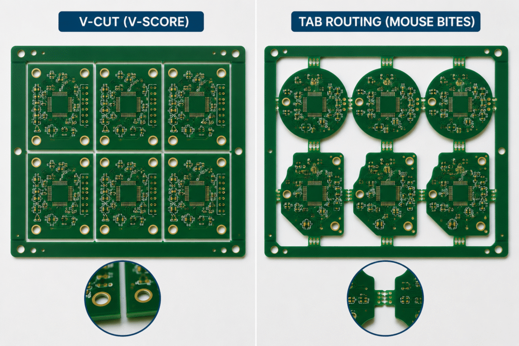
The table below compares V-Cut and tab routing from a PCB assembly perspective.
| Factor | V-Cut / V-Score | Tab Routing |
|---|---|---|
| Best For | Rectangular PCBs | Irregular PCB shapes |
| Board Edge | Straight edges | Complex outlines |
| Cost | Usually lower | May be higher |
| Panel Strength | Good for simple designs | Stronger support when designed well |
| Depaneling | Fast and simple | Requires tab removal or cutting |
| Edge Quality | Usually clean on straight edges | May leave mouse bite marks |
| Component Clearance | Important near score lines | Important near tabs |
| Design Flexibility | Limited | High |
| Production Efficiency | Good for volume production | Good for complex designs |
| Typical Use | Standard PCBA | Custom-shaped PCBA |
V-Cut is often better for simple rectangular boards and high-volume production.
Tab routing is often better for irregular board shapes, small boards, or products that need special mechanical fit.
The best choice depends on PCB geometry, assembly process, and final product requirements.
How PCB Panelization Affects Assembly Quality
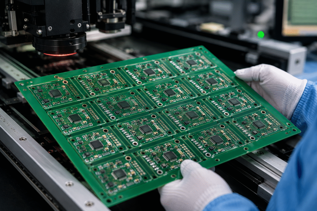
PCB panelization can affect production quality in several important ways.
Panel Rigidity
The panel must be rigid enough to pass through SMT equipment without bending or shifting.
If the panel is too weak, it may cause printing defects, placement errors, or reflow instability. This is especially important for thin PCBs, small boards, or panels with many routed openings.
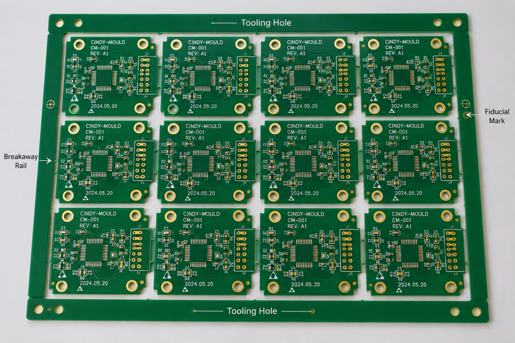
Fiducial Placement
Fiducial marks help SMT machines align the board accurately.
Poor fiducial placement can reduce placement accuracy, especially on panels with multiple boards. Global fiducials and local fiducials should be reviewed based on the PCB layout and assembly requirements.
Tooling Holes
Tooling holes help support accurate positioning during fabrication, assembly, inspection, and testing.
If tooling holes are missing or poorly placed, the panel may not align properly in fixtures or equipment. This can affect production repeatability.
Component Clearance Near Edges
Components should not be placed too close to V-Cut lines, tabs, mouse bites, or routed edges.
Insufficient clearance can increase the risk of component damage during depaneling. Connectors, ceramic capacitors, LEDs, and fine-pitch components near the board edge should be reviewed carefully.
Breakaway Rails
Breakaway rails provide extra support for small boards or boards with components near the edge.
They can help the panel move more smoothly through SMT equipment and make handling easier before depaneling.
Depaneling Method
The depaneling method should be considered before production.
Common methods include manual breaking, cutting, routing, and specialized depaneling equipment. The method should match the panel design and component sensitivity.
For high-reliability products, depaneling stress should be controlled carefully to reduce the risk of hidden solder joint damage. Inspection criteria and solder joint quality should also follow relevant IPC standards where applicable.
Common PCB Panelization Mistakes
Many panel-related issues can be avoided if the panel design is reviewed before production.
Components Too Close to the Panel Edge
This is one of the most common mistakes.
If components are placed too close to V-Cut lines or tabs, they may be damaged during depaneling. Even if there is no visible damage, mechanical stress may affect solder joints.
Weak Panel Support
A panel with too many cutouts or poorly placed tabs may become weak.
Weak panels can bend during printing, placement, or reflow. This may cause solder paste misalignment, component shift, or inconsistent solder joints.
Poor Fiducial Placement
Fiducials should be clear, accessible, and placed correctly.
If fiducials are too close to the edge, blocked by components, or inconsistent across the panel, SMT alignment may become less reliable.
Ignoring Depaneling Stress
Depaneling should not be treated as a final minor step.
If the separation method creates too much stress, it may damage components, solder joints, or board edges. This is especially important for products with connectors, ceramic components, or dense layouts near the edge.
Wrong Panel Direction
Panel orientation affects how the board moves through SMT equipment.
The wrong direction may reduce support, increase warpage, or make inspection and handling less efficient. Panel direction should be confirmed before mass production.
No Consideration for Testing Fixtures
If the board requires ICT, functional testing, or fixture-based testing, panelization should consider test point access and fixture positioning.
A panel that is good for SMT may still create problems during testing if access is not considered early.
What Buyers Should Confirm Before PCB Panelization
Before confirming PCB fabrication and assembly, buyers should review key panelization details with the supplier.
📌 Use this checklist before production:
- What is the final PCB size and shape?
- Is the board rectangular or irregular?
- Should the panel use V-Cut or tab routing?
- Are any components close to the board edge?
- Are connectors placed near the depaneling area?
- Is there enough clearance around V-Cut lines or tabs?
- Does the panel need breakaway rails?
- Are fiducials and tooling holes included?
- What depaneling method will be used?
- Will the board require AOI, ICT, or functional testing?
- Does the PCB need to fit into a plastic enclosure after assembly?
- Are there cost or production volume targets?
For buyers preparing files for quotation, a complete PCB Assembly RFQ Checklist can help reduce missing details and improve communication before production.
How PCB Panelization Affects PCBA Cost
PCB panelization can also affect the total PCBA cost.
A good panel design can improve production efficiency and reduce handling time. A poor panel design may increase manufacturing cost because of extra routing, difficult depaneling, lower yield, rework, or slower production.
Panelization can affect cost through:
- PCB fabrication process
- SMT production efficiency
- Panel utilization rate
- Depaneling method
- Inspection time
- Rework risk
- Labor requirements
- Scrap rate
For cost-sensitive projects, it is important to evaluate both PCB fabrication cost and assembly cost. A panel that looks cheaper during PCB fabrication may not always reduce the total project cost if it creates assembly or depaneling problems.
For buyers comparing quotations, this should be considered together with the full PCBA cost breakdown.
How Cindy Mould Supports PCB Panelization Review
At Cindy Mould, PCB panelization is reviewed as part of the complete electronics manufacturing process.
Instead of treating panelization as only a PCB supplier decision, we evaluate it together with the PCB layout, BOM, component placement, SMT process, testing requirements, and final product assembly.
Gerber and BOM Review
Before production, our team reviews the Gerber files and BOM to understand board size, shape, component package types, edge clearance, connector position, and possible assembly risks.
If the design includes small boards, irregular shapes, fine-pitch components, or edge-mounted connectors, the panelization method should be checked carefully before production.
SMT Assembly Process Evaluation
Panelization affects solder paste printing, pick-and-place accuracy, reflow stability, AOI inspection, and depaneling.
By reviewing the complete assembly process, we help reduce avoidable production risks and improve PCBA consistency.
Testing and Fixture Consideration
For products that require AOI, ICT, or functional testing, panelization should support test point access and fixture compatibility.
If testing requirements are considered too late, the panel may need to be redesigned, causing delays and extra cost.
Product Assembly Compatibility
For custom electronic products, the PCB does not work alone. It must fit into the enclosure, connect with wires, align with buttons or displays, and support final product assembly.
That is why panelization should be reviewed together with the final product structure, not only the bare PCB.
Prototype and Small-Batch Support
Prototype and small-batch production are useful stages for checking whether the panel design works well before mass production.
If a panel causes handling issues, edge defects, or depaneling stress, these problems should be found early before larger production begins.
For projects involving custom PCBA, plastic enclosures, testing, and assembly, Cindy Mould can support custom electronics development from prototype to small-batch production.
Conclusion
PCB panelization affects much more than PCB fabrication efficiency.
It can influence:
- Solder paste printing
- SMT placement accuracy
- Reflow stability
- Inspection consistency
- Depaneling stress
- Edge quality
- Testing access
- Total PCBA cost
V-Cut is often suitable for rectangular boards, straight edges, and cost-sensitive volume production. Tab routing is often better for irregular board shapes, small boards, or designs that require stronger support and more flexible panel layouts.
The best PCB panelization method depends on board shape, component placement, panel strength, depaneling method, testing requirements, and final product assembly needs.
If you are not sure whether V-Cut or tab routing is better for your project, Cindy Mould can review your Gerber files, BOM, assembly requirements, and product structure before production.
FAQ
What is PCB panelization?
PCB panelization is the process of arranging multiple individual PCBs into one larger production panel. It helps improve SMT assembly efficiency, handling stability, inspection consistency, and production repeatability.
What is the difference between V-Cut and tab routing?
V-Cut uses straight scored lines to separate rectangular boards, while tab routing uses routed gaps and small tabs to hold boards in place. V-Cut is usually better for straight-edged boards, while tab routing is better for irregular shapes.
Is V-Cut better than tab routing?
V-Cut is not always better. It is efficient and cost-effective for rectangular PCBs, but it may not be suitable for irregular shapes or components placed near the board edge. Tab routing offers more flexibility for complex board designs.
When should I use tab routing?
Tab routing is suitable for irregular PCB shapes, small boards, curved outlines, boards with cutouts, or designs that need stronger panel support during SMT assembly.
Does PCB panelization affect SMT assembly quality?
Yes. PCB panelization can affect solder paste printing, pick-and-place accuracy, reflow stability, AOI inspection, depaneling stress, and final PCBA quality.
Can poor panelization increase PCBA cost?
Yes. Poor panelization can lead to extra routing, difficult depaneling, lower yield, more rework, slower production, or higher labor cost. A good panel design can help reduce total PCBA cost.