Introduction: The Hidden Risks of Ignoring DFM
DFM reduces electronic manufacturing risks for hardware startups that achieve flawless functionality in the prototype phase but face severe challenges during mass production.Low yields, high rework rates, warped injection-molded parts, and even complete mold failures are common problems that can delay product launches by weeks or months and cost tens of thousands of dollars.
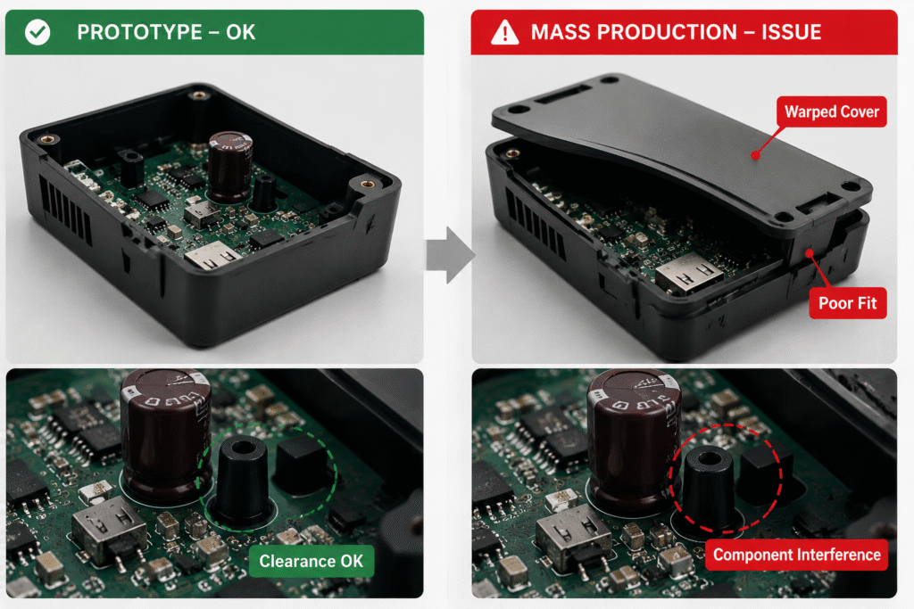
For example, a consumer electronics startup might find that vertical electrolytic capacitors on their PCB prevent the enclosure from closing correctly. Another case is where uneven wall thickness in injection-molded parts causes warpage, resulting in misaligned buttons or snapped connectors. According to industry reports, nearly 30% of PCB rework is due to unoptimized design or overlooked manufacturing constraints.
These challenges highlight the importance of Design for Manufacturing (DFM). DFM is not just a checklist or final drawing review—it is a proactive methodology that evaluates manufacturability at the earliest stage. By anticipating potential issues in both electronic and mechanical design, DFM ensures that products are ready for production without costly iterations.
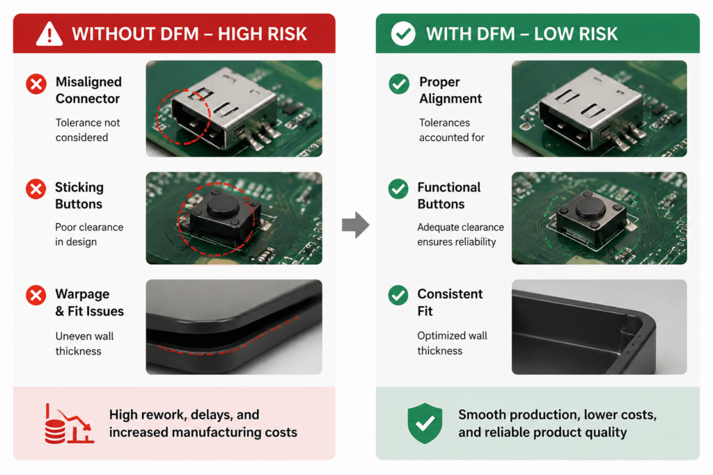
Consider a scenario where a prototype works perfectly in testing, but during assembly, minor tolerances cause connectors to misalign or buttons to stick. Without DFM, such issues often remain undetected until mass production, resulting in expensive rework or even mold scrapping.
By integrating DFM early, companies can prevent failures, optimize costs, and achieve reliable production. DFM acts as a bridge between creative design and factory realities, transforming potential manufacturing headaches into controlled, predictable outcomes.
Key takeaway: A robust DFM process is the first line of defense in ensuring smooth production, reducing material waste, and safeguarding both time and budget.
Why DFM Reduces Electronic Manufacturing Risks in One-Stop Manufacturing
Breaking Down Silos
One of the biggest challenges in electronics product development is the separation of electronic and mechanical design teams. DFM reduces these production risks by identifying potential conflicts early. PCBA engineers focus on circuit layout, while mechanical engineers focus on enclosures and molds. Without coordinated DFM, this siloed approach can lead to:
- Components that are physically too tall to fit within the enclosure
- PCB layouts that complicate automated assembly
- Insufficient spacing for thermal management or testing access
A one-stop EMS provider, such as CINDY-Mould, addresses this by aligning electronic, mechanical, and test engineers from the earliest design stage. By reviewing PCBA layouts alongside enclosure and mold designs, DFM reduces errors and prevents costly production issues before prototypes are built.
The Cost Leverage Principle
Statistics indicate that 70–80% of a product’s cost is determined during the design phase. DFM reduces these potential cost overruns by identifying and correcting design issues early. Correcting errors at the design stage typically costs $1–$5 per issue, while fixing the same problem after mass production can exceed $10,000 per incident. Early DFM reviews are therefore a high-leverage cost-saving measure that ensures DFM reduces overall production risks.
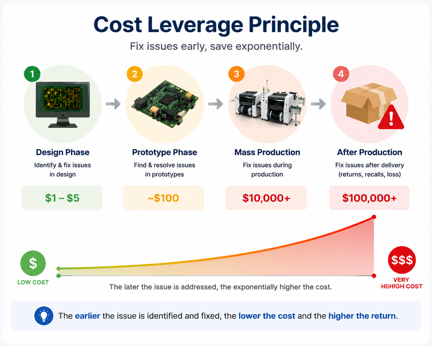
| Stage | Cost per Error | Typical Impact |
|---|---|---|
| Design Phase | $1–$5 | Easily corrected in CAD |
| Prototype | ~$100 | Minor rework required |
| Mass Production | $10,000+ | Delays, rework, mold scrapping |
Enhancing Reliability and Yield
DFM ensures higher production reliability and DFM reduces assembly errors by:
- Increasing SMT assembly yield through optimized PCB layouts
- Reducing mold rework and scrap in injection-molded parts
- Ensuring smooth functional testing (FCT) and automated optical inspection (AOI)
- Optimizing panelization to reduce material waste
By addressing potential manufacturing challenges early, DFM reduces risks and directly impacts cost efficiency, product reliability, and time-to-market.
Cindy-Mould’s One-Stop Advantage
Cindy-Mould coordinates PCBA design, injection molding, and testing in a single workflow. By having engineers review all aspects together, the company ensures:
- Mechanical constraints are considered in electronic design
- Electronic layout accommodates enclosure tolerances
- Potential issues are identified before prototypes are built
This integration prevents downstream delays and enhances client confidence in both design and manufacturability.
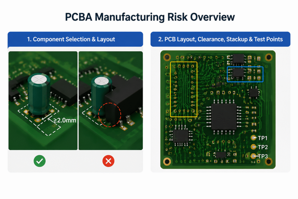
How DFM Reduces Production Issues in PCBA Manufacturing
Component Selection and Availability
The choice of components affects both assembly and supply chain reliability:
- End-of-Life (EOL) Components: Avoid using parts that may soon be discontinued to prevent supply chain disruptions.
- Footprint Compatibility: SMT pad sizes must match automated pick-and-place machines; incorrect sizes reduce yield.
- Thermal Considerations: Components must withstand soldering temperatures to avoid defects such as tombstoning or lifting.
Tip: Prefer industry-standard, widely available components and verify footprints using CAD libraries.
Routing, Spacing, and Layer Stack
PCB trace width, spacing, and stack design influence manufacturability and signal integrity:
- Narrow traces increase the risk of shorts and EMI interference.
- High-speed or high-frequency signals require impedance control.
- Layer stack design affects thermal dissipation and manufacturability.
SMT (Surface Mount Technology): Components are mounted directly on PCB pads using automated machines. Proper pad design ensures soldering quality and reduces defects.
Design for Test (DFT)
Functional testing is essential to detect defects before assembly completion:
- AOI (Automated Optical Inspection): Detects soldering defects, missing components, and misalignment.
- ICT (In-Circuit Test): Checks electrical continuity and component functionality.
- FCT (Functional Circuit Test): Verifies full PCB functionality under operational conditions.
Failing to plan test points can result in inaccessible measurement locations, making defects hard to detect and increasing rework.
Panelization
Panelization combines multiple PCBs onto a single panel for efficient assembly:
- Reduces material waste
- Simplifies handling during solder paste application and automated assembly
- Allows simultaneous testing and inspection
Proper panelization is critical to achieving high yield, minimizing cost, and streamlining mass production.
Thermal Management and Signal Integrity
- Thermal reliefs for heat-sensitive components prevent damage during soldering.
- Ground planes and shielding reduce EMI for sensitive analog or RF circuits.
- Via stitching ensures consistent grounding and reduces signal noise.
Incorporating these factors into DFM ensures higher functional yield and long-term reliability.
Injection Molding and Mold DFM: Mitigating Risks
Wall Thickness Uniformity
DFM reduces the risk of defects in injection-molded parts by addressing uneven wall thickness, draft angles, and gate placement before production.
Uneven wall thickness can cause:
- Sink marks and surface imperfections
- Warpage affecting assembly
- Uneven shrinkage that misaligns components
Applying DFM reduces the likelihood of warpage and sink marks by ensuring uniform wall thickness. For electronic enclosures, uniform wall thickness ensures structural integrity and aesthetic consistency. Recommended wall thickness depends on material: 1.2–3.0 mm for ABS/PC parts is common.
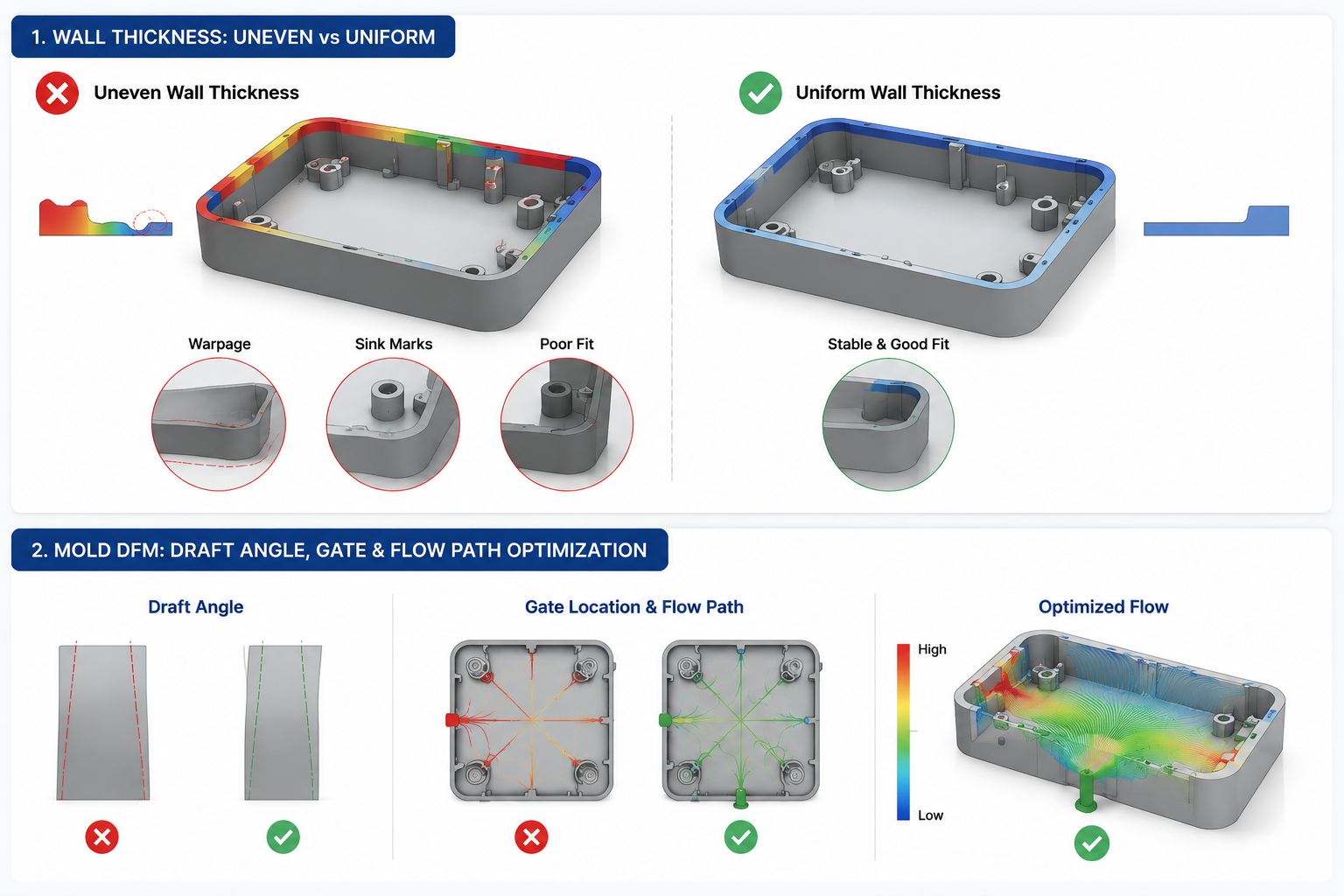
Draft Angles
Draft angles facilitate smooth ejection from molds:
- Insufficient draft causes scratches, torn edges, or broken features
- Standard angles range from 1–2°, adjusted for material and feature geometry
Gate Placement and Flow Path
Proper gate location and flow path design prevent:
- Weld lines or visible seams
- Voids or weak points in the structure
- Inconsistent surface finish
Optimized flow reduces rework and ensures high-quality finishes.
Tolerance Chain Analysis
Tolerance considerations are critical when combining PCBA with enclosures:
- Misjudged tolerances can prevent PCB fitting
- Cumulative tolerance errors affect button and connector alignment
- Incorporating material shrinkage and assembly clearances is essential
Tip: Use CAD simulations to model tolerance stack-up before production.
Material Selection
Material choice affects manufacturability:
- ABS: Good impact resistance and surface finish
- PC: Higher heat resistance, suitable for electronics housings
- PA (Nylon): Strong, may absorb moisture affecting dimensions (injection molding material guide)
Selecting the right material reduces defects and improves reliability.
Case Mini-Example
During DFM review, Cindy-Mould engineers discovered a design where wall thickness variation and misaligned ejector pins could lead to warp. Adjustments prevented mold rework and ensured smooth assembly, saving both time and cost.
Case Study: How DFM Reduces Costs and ReworkCase Study: Avoiding Costly Rework
Background: A smart home electronics client provided a prototype with vertical electrolytic capacitors on the PCB.
Challenge: Capacitors prevented enclosure closure, risking mold rework and assembly failure.
Solution:
- Replaced vertical capacitors with side-mounted versions
- Adjusted mold ejector pin positions
- Verified PCB alignment within enclosure tolerances
Results:
- Avoided a second mold creation, saving 4 weeks and $30,000+
- Improved assembly yield and reduced functional test failures
- Strengthened client confidence in design and production reliability
This case demonstrates how applying DFM reduces production delays and prevents costly rework.
Comparative Table: With DFM vs Without DFM
| Metric | With DFM | Without DFM |
|---|---|---|
| Development Time | Optimized | Frequent delays |
| Mold Rework | Rare | Common, costly |
| PCB Assembly Yield | High | Low |
| Functional Testing | Smooth | Blocked or delayed |
| Material Waste | Minimal | Higher |
| Product Launch Delay | Minimal | Weeks or months |
| Customer Satisfaction | High | Risk of complaints |
Conclusion & Call to Action
DFM is not an extra cost—it is the most effective insurance for electronic manufacturing. Early integration of DFM prevents delays, improves yield, reduces rework, and ensures consistent product quality.
Call to Action:
Don’t let your product face avoidable manufacturing risks. Contact Cindy-Mould’s engineering team for a free DFM assessment and ensure your design transitions smoothly from prototype to mass production.
FAQ
Q1: When should DFM start?
- At the earliest design stage to prevent costly downstream errors.
Q2: Does DFM restrict creativity?
- No. It guides feasible designs without limiting innovation.
Q3: What is Cindy-Mould’s DFM process?
- Integrated review of PCB layout, component selection, mold design, tolerance analysis, and test point planning.
Q4: Can DFM reduce production defects?
- Yes. Early detection improves yield and reduces field failures.
Q5: How does DFM impact cost?
- Saves money by reducing rework, scrap, and mold modifications.
Q6: Is DFM only for high-volume production?
- No. Small-batch or prototype products also benefit from early DFM.
Q7: How are PCB tolerances verified?
- CAD simulations and tolerance stack-up analysis are performed to ensure fit and function.
Q8: What role does material selection play in DFM?
- Material properties affect shrinkage, warpage, and thermal stability, influencing manufacturability.