Introduction
Where Electrical Design Meets Mechanical Structure
PCB enclosure integration is a critical challenge in modern electronics product development. Modern electronics products rarely rely on a single engineering discipline. Instead, they are developed through the collaboration of electrical engineering, mechanical design, tooling development, and manufacturing engineering.
Within this multidisciplinary environment, one of the most important engineering interfaces occurs between the PCB and the product enclosure. Effective PCB enclosure integration ensures that electrical design and mechanical structures work together smoothly during product assembly and mass production.
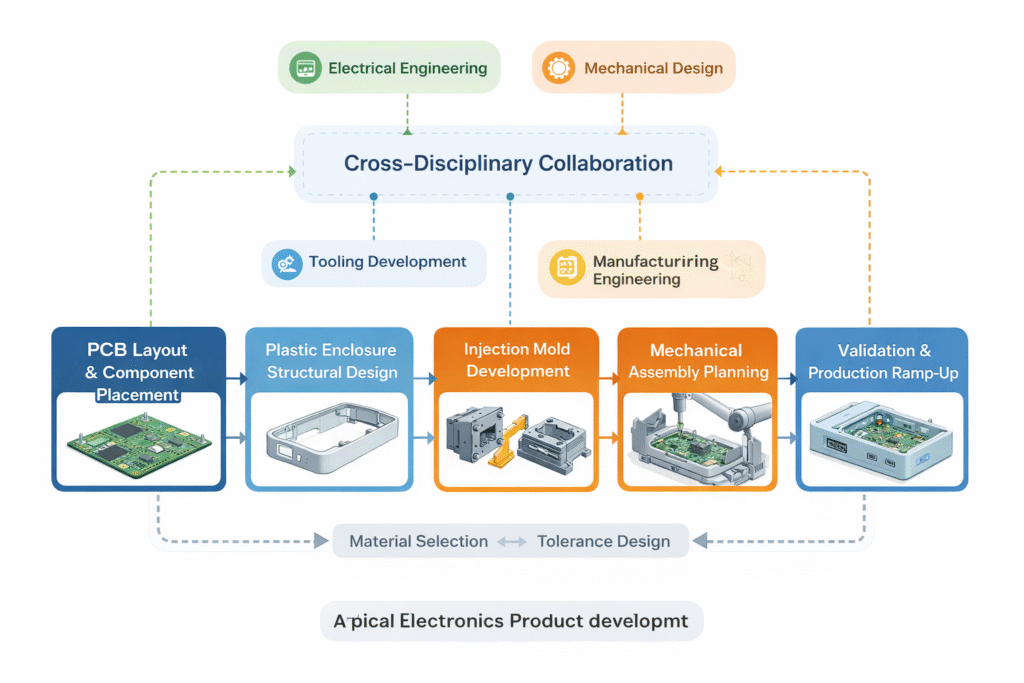
A typical electronics product involves several interconnected design stages:
- PCB layout and component placement
- plastic enclosure structural design
- injection mold development
- mechanical assembly planning
- validation and production ramp-up
Each of these processes introduces its own design considerations, dimensional tolerances, and engineering constraints.
Electrical engineers primarily focus on signal routing, component functionality, and circuit performance. Mechanical engineers, on the other hand, must ensure that the PCB can be securely mounted inside the product housing while maintaining structural stability and assembly accessibility.
When these disciplines are developed independently, PCB enclosure integration issues often appear during prototype builds or early production stages.
These challenges are rarely caused by individual design mistakes. More often, they result from small misalignments between electrical and mechanical design assumptions.
Understanding how PCB structures interact with plastic enclosures is therefore essential for achieving reliable PCB enclosure integration in electronics products.
Key Interfaces in PCB Enclosure Integration
PCB boards and plastic housings interact at several critical structural interfaces during assembly.
Some of the most common PCB enclosure integration interfaces include:
- PCB mounting holes and enclosure screw bosses
- connector positions and enclosure openings
- component height and enclosure internal clearance
- cable routing and internal structural obstacles
- thermal expansion between different materials
Each of these interfaces introduces potential dimensional interaction between electrical and mechanical systems.
Even when every individual component is designed within specification limits, the combined interaction between these systems can create unexpected assembly challenges.
In many cases, PCB enclosure integration problems only become visible when the PCB and enclosure are physically assembled together during prototype testing.
PCB Mounting Alignment and Boss Design
One of the most frequent PCB enclosure integration challenges appears at the interface between PCB mounting holes and enclosure screw bosses.
PCBs are typically designed with mounting holes positioned according to strict electrical and mechanical requirements. These holes must align precisely with corresponding bosses or standoffs inside the plastic enclosure.
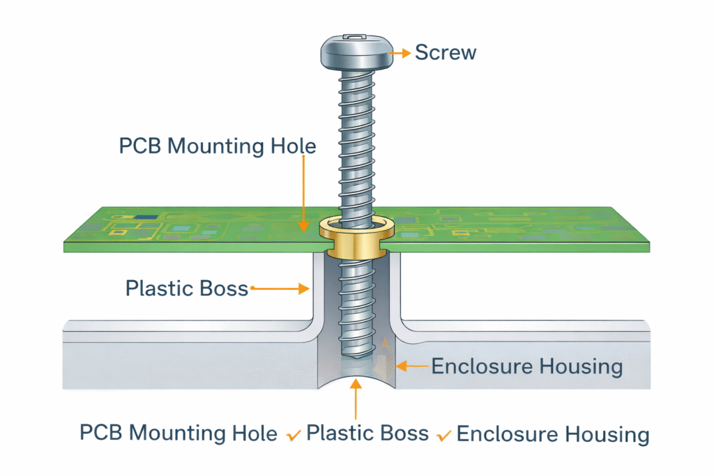
However, injection molded plastic housings naturally include dimensional variation caused by several factors:
- mold machining tolerances
- material shrinkage during cooling
- wall thickness variation
- molding process stability
Meanwhile, PCB manufacturing also includes positional tolerances for drilling and board fabrication.
When these tolerances accumulate, the PCB mounting holes may not perfectly align with the enclosure bosses during assembly.
In such cases, assembly operators may need to apply additional force to insert screws or slightly reposition the PCB to complete the assembly process.
Although these adjustments may appear minor, repeated mechanical stress can influence product reliability over long production cycles.
These dimensional interactions are often closely related to tolerance stack-up, where small variations from multiple components accumulate during assembly.
Connector Position and Enclosure Interface Design
Connector positioning is another critical area affecting PCB enclosure integration.
During PCB layout design, connectors are placed according to signal routing requirements, electrical spacing rules, and component layout constraints.
However, these connectors must also align with openings in the plastic enclosure that allow user access to external interfaces.
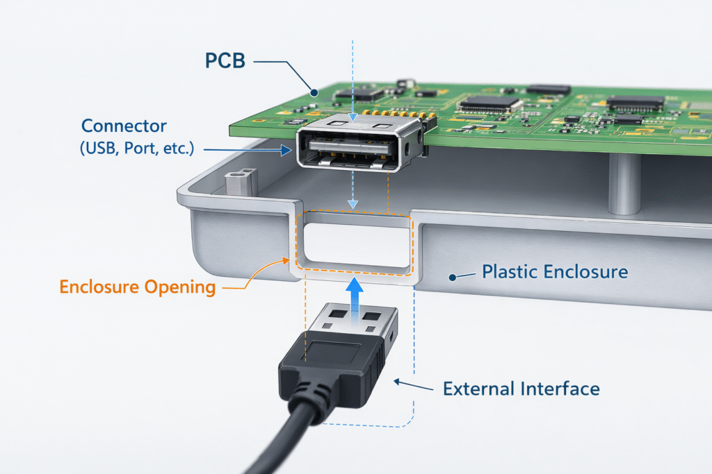
Common examples include:
- USB connectors
- charging ports
- audio jacks
- power input connectors
- communication interfaces
If connector placement is not coordinated with enclosure design, several practical assembly problems may appear.
Connectors may sit slightly recessed inside the housing, making them difficult to access. In other cases, connectors may press against the enclosure wall, creating mechanical stress on solder joints.
Even small positional differences can affect how cables or plugs interact with the connector interface.
These issues are frequently discovered only during prototype assembly, when the PCB is installed inside the enclosure for the first time.
Early cross-disciplinary review between electrical and mechanical teams can significantly improve PCB enclosure integration quality and reduce these risks.
Component Height and Internal Clearance Constraints
Component height is another important factor influencing PCB enclosure integration.
Electronic components such as electrolytic capacitors, connectors, shielding cans, transformers, and heat sinks may extend significantly above the PCB surface.
At the same time, plastic housings often include internal structures designed for strength and assembly stability, such as:
- reinforcing ribs
- mounting posts
- snap-fit features
- cable guides
- thermal support structures
If component height is not coordinated with enclosure design, physical interference may occur when the enclosure is closed during assembly.
These conflicts can prevent proper enclosure sealing or introduce pressure on sensitive components.
Resolving these issues often requires redesigning the enclosure structure, relocating PCB components, or adjusting internal clearances.
When discovered late in development, such modifications can delay tooling development and increase project cost.
Thermal Expansion and Material Interaction
Material interaction is another factor that influences PCB enclosure integration performance.
PCBs, plastic housings, and metal components all expand differently under temperature variation.
For example:
- FR-4 PCB material has its own thermal expansion characteristics
- plastic housings may expand or contract depending on resin type
- metal brackets may behave differently under thermal stress
When these materials interact within a tightly constrained product structure, thermal expansion differences may introduce additional stress on mounting points and connectors.
In extreme cases, repeated thermal cycling can gradually influence structural alignment or mechanical stability.
Careful material selection and structural tolerance design can help minimize these long-term reliability risks.
Preventing Integration Issues Through Early Coordination
Many PCB enclosure integration challenges can be prevented through early engineering coordination.
Instead of designing electrical and mechanical systems independently, development teams should evaluate the product structure as a unified assembly system.
Several practices can help reduce integration risk:
- early cross-disciplinary design reviews
- 3D CAD assembly verification
- tolerance analysis between structural components
- early involvement of tooling engineers
These practices allow engineers to identify dimensional conflicts before production tooling is finalized.
Early coordination also helps reduce the number of engineering changes required during the later stages of product development.
Key Takeaways
PCB enclosure integration is a critical aspect of electronics product development.
Important considerations include:
- precise alignment between PCB mounting holes and enclosure bosses
- connector positioning relative to enclosure openings
- component height compatibility with enclosure internal space
- dimensional variation caused by manufacturing tolerances
- material interaction during temperature variation
When electrical and mechanical designs are developed in isolation, PCB enclosure integration issues often appear during prototype assembly or early production.
However, when engineering teams collaborate early in development, many of these challenges can be identified and resolved before they affect manufacturing.
Conclusion
Integration Quality Determines Manufacturing Stability
In electronics manufacturing, product stability depends not only on individual component performance but also on how well different engineering systems interact.
The relationship between PCB design and plastic enclosure design clearly illustrates the importance of effective PCB enclosure integration.
Even when each component meets its own design specifications, small dimensional differences between electrical and mechanical systems can create assembly challenges during production.
By improving collaboration between electrical engineers, mechanical designers, and manufacturing teams, companies can significantly reduce integration risks and improve overall manufacturing stability.
In complex electronics products, successful manufacturing is ultimately the result of well-coordinated engineering decisions across the entire product structure.