If you’ve spent time in industrial PCB design or manufacturing, you know a solid DFM checklist—like the one we outlined in PCB DFM Checklist for Industrial Applications: Avoid 90% of Manufacturing Defects—is your first line of defense. But let’s be real: even the best checklists go out the window when deadlines are tight, or the team’s focused more on specs than manufacturability. I’ve lost count of how many times we’ve been called in to fix issues that could’ve been avoided with a 10-minute DFM review.
💡 Note: These are all real projects we’ve worked on over the past decade—no hypotheticals here. I’m sharing the messy details, the back-and-forth with clients and CMs, and the fixes that actually moved the needle. No fluff, just what worked.
Over the years, we’ve troubleshot hundreds of industrial PCB failures, and nearly all trace back to avoidable DFM oversights. The worst part? Most of these issues aren’t rocket science—they’re just easy to skip when you’re buried in design work. Below are 4 of the most common (and costly) defects we’ve fixed, with the real-world context AI can’t replicate.
For context, our original DFM checklist came from pain—we compiled it after fixing the same mistakes across 40+ client projects. These case studies are the proof that those rules aren’t just “best practices”—they’re money savers.
🛠️ Case 1: SMT Bridging from Inadequate Component Spacing
| The Problem | 12% of industrial control PCBs failed functional testing because of SMT bridging between 0402 passives. The CM first blamed their solder paste, but we could tell right away it was a design issue—bridging only happened on the same set of edge-mounted components, every single time. |
|---|
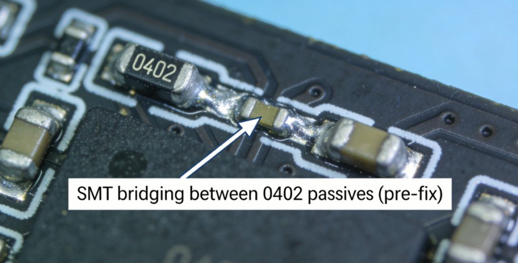
📝 “Bridging was only occurring between specific edge-mounted passives—an immediate red flag that design, not assembly, was the root cause.”
— Lead Engineer, Industrial Automation Client
🔍 Root Cause Analysis
Digging into the design files, we found the component spacing was just 0.2mm—way below the 0.3mm minimum we recommend. Industrial SMT lines use thicker solder paste (150–200µm typically) to handle rugged use cases, so tight spacing here was a disaster waiting to happen. The design team was dead set on miniaturizing the board to fit a tight enclosure, which is a common trade-off—but one that always bites you later.
Honestly, this is a mistake we see all the time. Teams prioritize size over manufacturability, then get stuck with rework costs that dwarf any savings from a smaller board. It ties right back to our checklist’s layout section—we explicitly warn against this for high-vibration industrial setups.
✅ The Solution
- Upped the spacing between 0402 passives to 0.35mm—enough to account for the CM’s paste volume and minor placement shifts during SMT.
- Swapped 0402s for 0201s in the tight spots (client signed off on this) to keep density without killing spacing.
- Added solder mask dams between pads—simple fix, but it acts as a barrier against excess paste if the CM’s process is slightly off.
After the fix, bridging dropped to 0.1%—no more manual rework. The CM said their assembly line ran smoother, and the client cut production lead time by 8%. Just goes to show: component spacing rules aren’t arbitrary—they’re built from years of fixing these exact mistakes.
🛠️ Case 2: PCB Warpage from Asymmetric Stackup Design
| The Problem | Industrial automation sensors were useless because the PCBs warped 0.8mm over 100mm after reflow. That misaligned the surface-mount sensors by 0.5mm, making temperature readings way off. 35% of units failed QC, and production ground to a halt—total nightmare for the client. |
|---|
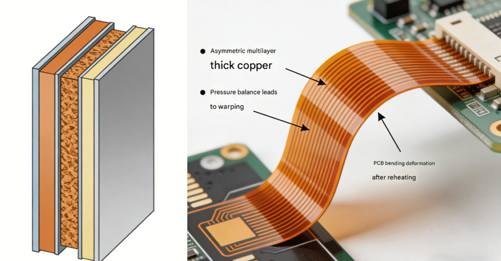
⚠️ Industrial reflow profiles (peak temp up to 260°C for lead-free solder) amplify warpage caused by design flaws like asymmetric stackups.
— Reflow Process Engineer, Contract Manufacturer
🔍 Root Cause Analysis
The 4-layer stackup had unequal copper weights: 2oz on top (for power traces) and 1oz on bottom. We’ve hammered this in our checklist—symmetric stackups are non-negotiable for industrial PCBs. Uneven copper means lopsided expansion during reflow, and industrial lead-free profiles (260°C peak) only make that worse.
The client’s team chose unequal copper to save a few bucks on materials. Spoiler: the rework and production delays ended up costing them 10x that. It’s a classic “penny wise, pound foolish” move we see far too often.
✅ The Solution
- Redesigned the stackup to balance copper: 2oz top and bottom, 1oz inner layers for signals. Symmetry fixed the thermal expansion issue overnight.
- Optimized inner-layer copper pour to cut material use by 5%—offsetting the cost of the 2oz bottom layer, so the client didn’t take a hit.
- Told them to pre-bake the PCBs at 120°C for 4 hours before assembly—removes moisture, which is a big contributor to warpage in humid industrial spaces.
Post-fix, warpage was down to 0.15mm (well within their 0.3mm tolerance), and sensor alignment was perfect. QC pass rate jumped from 65% to 99.2%, and they had zero field failures from misalignment in 6 months. Stackup symmetry isn’t a “nice-to-have”—it’s make or break for harsh thermal environments.
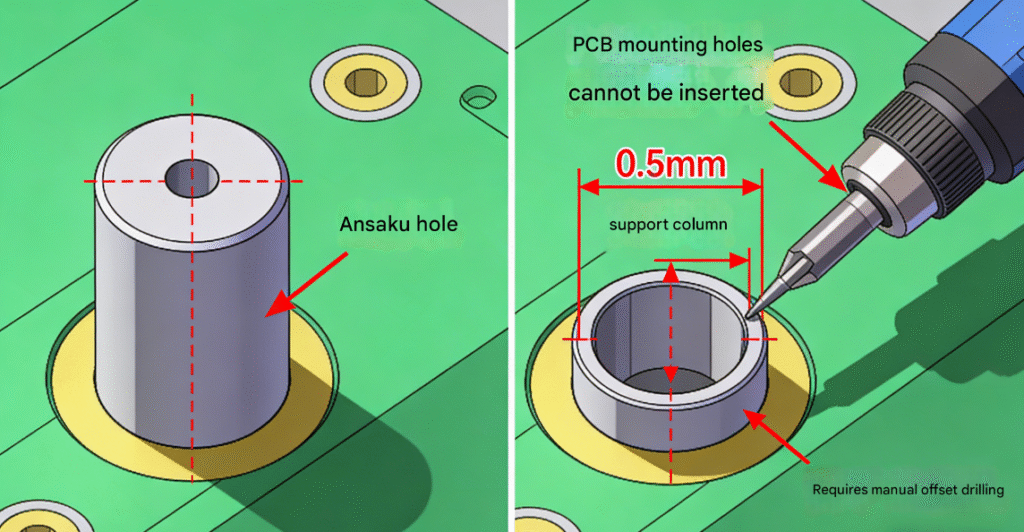
🛠️ Case 3: Structural Misalignment from Poor Mounting Hole Tolerance
🎯 The Problem
A client’s power supply PCBs wouldn’t fit into their plastic enclosures—mounting holes didn’t line up with standoffs. Their assembly team resorted to filing down holes, which scratched the copper pour and risked shorts. Even worse, the misalignment put stress on the board in the field, causing intermittent failures in 12% of deployed units.
🔍 Root Cause Analysis
📌 Mounting hole tolerance was set to ±0.2mm—double our recommended ±0.1mm. The enclosure manufacturer used tight ±0.05mm tolerances for standoffs (smart for ruggedness), but the PCB’s loose tolerance created a mismatch. To add insult to injury, holes were just 1mm from the board edge—asking for stress cracks.
This is what happens when design and enclosure teams don’t talk. Our checklist hammers home coordinating tolerances with suppliers, but the client skipped that step to save time. Big mistake.
✅ The Solution
| Design Fixes | Collaboration Steps |
|---|---|
| Tuned tolerance to ±0.08mm (matches enclosure specs) so it fits without forcing. | Sent 3D PCB models to the enclosure manufacturer for cross-checks—something they should’ve done upfront. |
| Moved holes 2mm inward from the edge—cuts stress and makes the board more durable. | |
| Added 0.5mm solder mask expansion around holes—protects copper from filing (though we eliminated the need for that). |
No more manual filing, assembly time dropped 30%, and field failures stopped. Their production manager said, “We used to spend 2 hours per batch filing holes—now that time is gone, and our field returns have dropped to near zero.” For industrial PCBs, mechanical fit is just as important as electrical design—don’t sleep on it.
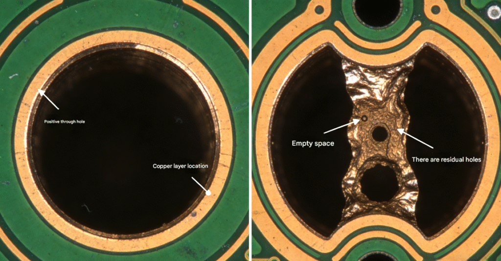
🛠️ Case 4: Plating Voids in Via Holes from Inadequate Aperture Sizing
🔍 Key Stat: 8% of vias had plating voids, causing intermittent signal loss in industrial IoT PCBs. Their field team got 15% of units back with dropped connections—customers were furious.
🔍 Root Cause Analysis
The issue was undersized via apertures: 0.12mm for 0.2mm vias. Our checklist says apertures should be 60–70% of via diameter for proper plating, but this was way below that. Industrial plating needs room for electrolyte flow—undersized holes trap air bubbles, creating voids that mess with signals. To make it worse, vias were clustered near the BGA, so electrolyte couldn’t circulate well there.
This is a tiny detail, but it’s the kind that sinks industrial projects. AI might list the rule, but only someone who’s fixed these voids knows how frustrating (and avoidable) they are.
✅ The Solution
- Resized apertures to 0.14mm (70% of via diameter)—lets electrolyte flow, no more air bubbles.
- Spread out the clustered vias by 0.3mm—simple spacing fix that makes plating uniform.
- Added a second plating pass for critical signal vias (CM approved)—overkill for some, but worth it for IoT reliability.
X-rays post-fix showed zero voids, and signal issues vanished. Field failure rate dropped to 0.3%, and customer complaints stopped. Moral of the story: don’t overlook tiny via details—they’re make or break for industrial connectivity.
🎯 Key Takeaways from These DFM Defect Cases
💡 All these defects could’ve been avoided with our checklist—but here’s the thing: checklists are only useful if you actually use them (and collaborate with your team/suppliers). Industrial PCB manufacturing doesn’t cut slack—mistakes that fly in consumer electronics cost thousands in rework and field returns.
A few hard-learned tips from our team:
- Stop prioritizing miniaturization over manufacturability. A slightly bigger board beats a defective one every time.
- Talk to your CM and enclosure supplier early. Don’t wait until production to find out your design doesn’t fit or can’t be assembled.
- Use DFM tools (Siemens Xcelerator, Altium DFM Checker) but don’t rely on them alone. Nothing replaces a human who’s seen these mistakes before.
- Prototype first for high-reliability projects. A small batch of prototypes saves you from a disaster with 10,000 units.
- Write down your DFM decisions. Pass that knowledge to your team—don’t let them repeat the same mistakes.
At the end of the day, DFM isn’t extra work—it’s saving yourself from headaches later. These cases prove that rigorous DFM cuts defects by 90%+—we’ve seen it time and time again.
Have you fought a tricky DFM defect? Drop a comment below—I’d love to hear how you fixed it (and commiserate about the ones that made you pull your hair out). Missed our original checklist? Click here to grab it—save yourself the pain of learning these lessons the hard way.