In industrial electronics manufacturing, printed circuit boards (PCBs) serve as the core of product operation. However, statistics show that over 60% of PCB manufacturing defects stem from inadequate Design for Manufacturability (DFM) considerations. Especially for high-complexity products like 6-layer PCBs widely used in industrial control and automotive electronics, neglecting DFM rules can lead to prolonged production cycles, increased rework costs, and even compromised product reliability.
This article compiles a practical DFM checklist tailored for industrial-grade PCBs, covering stackup design, layout specifications, process compatibility, and structural matching. By following this checklist, electronic design engineers can effectively reduce defect rates, ensure smooth mass production, and achieve seamless integration with subsequent processes such as SMT (Surface Mount Technology) and plastic enclosure assembly. Our one-stop service, integrating PCB design, plastic molding, and whole-machine assembly, further helps enterprises bridge the gap between design and manufacturing.
1. Stackup Design DFM Checklist: Balance Performance and Manufacturability
Stackup design is the foundation of PCB performance and manufacturability. For industrial PCBs with different layer counts (4-layer, 6-layer, 8-layer), the following DFM criteria must be strictly followed:
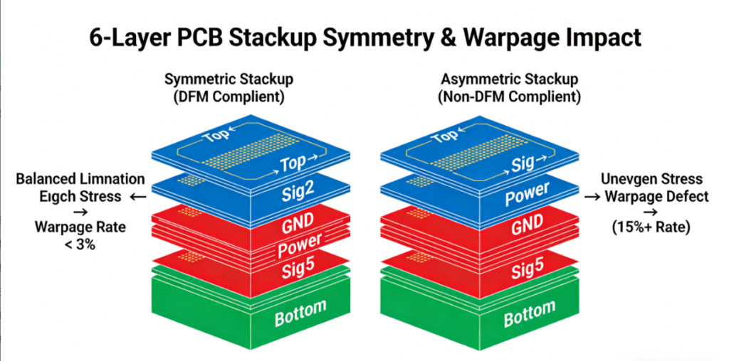
- Symmetry Check: The stackup structure must be symmetric relative to the central layer. For 6-layer PCBs, the standard symmetric stackup is Top Layer → Signal Layer 2 → GND Layer → Power Layer → Signal Layer 5 → Bottom Layer. Asymmetric stackup will cause uneven stress during lamination, leading to PCB warpage, a common defect in industrial applications.
- Copper Thickness Matching: The copper thickness of each layer should match the manufacturing process capabilities. For industrial control PCBs requiring high current carrying capacity, the copper thickness of power layers should be ≥2oz, while signal layers can use 1oz copper. It is crucial to confirm with manufacturers the maximum and minimum copper thickness tolerances to avoid excessive etching or insufficient current capacity.
- Substrate Selection: Choose substrates based on industrial operating environments. For high-temperature industrial scenarios (e.g., automotive engine compartments), use high-Tg substrates (Tg ≥170℃) to prevent substrate deformation. For humid environments, select substrates with good moisture resistance to avoid delamination.
- Dielectric Layer Thickness Control: The thickness of dielectric layers between signal layers and power/GND layers should balance signal integrity and manufacturability. For 6-layer PCBs, the dielectric layer thickness between adjacent layers is recommended to be 0.15-0.2mm, which is compatible with standard lamination processes and ensures effective impedance control.
2. Layout DFM Checklist: Key Specifications for Industrial PCB Production
Layout defects are the primary cause of SMT (Surface Mount Technology) failures and short circuits in industrial PCBs. The following quantitative DFM rules should be integrated into the layout design process:
- Component Spacing Requirements: The minimum spacing between adjacent components should be ≥0.5mm for standard components (0402, 0603) and ≥1.0mm for large components (e.g., connectors, inductors). This ensures sufficient space for SMT stencil printing and reflow soldering, avoiding solder bridging.
- Pad Dimension Standards: Pad dimensions must match component footprints. For 0603 resistors, the recommended pad length is 1.2mm and width is 0.6mm; for QFP components, the pad pitch tolerance should be ≤±0.02mm. Avoid oversized or undersized pads, which can lead to poor solder joints or component detachment in vibration-prone industrial environments.
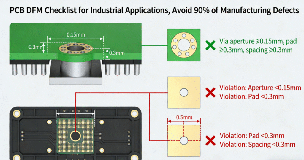
- Via Layout Taboos: For 6-layer PCBs, through-hole vias should have an aperture ≥0.15mm and pad diameter ≥0.3mm. The minimum spacing between adjacent vias is ≥0.3mm to prevent plating voids during electroplating. Never place vias on component pads or within 5mm of the PCB edge, as this can cause solder inflow or edge chipping during depaneling.
- Copper Pouring Guidelines: Copper pouring should be uniform across the PCB to reduce thermal stress. For industrial PCBs with high power consumption, add proper thermal relief pads to connect copper pours with component pads, ensuring heat dissipation while avoiding cold joints caused by excessive heat absorption during soldering.
3. Process Compatibility DFM Checklist: Align with SMT and Assembly Processes
Industrial PCB production involves multiple processes, and DFM design must ensure compatibility with SMT贴片, reflow soldering, wave soldering, and depaneling processes:
- SMT Stencil Compatibility: For BGA components, the stencil opening should adopt a laser-cut stepped design to ensure sufficient solder paste volume. For fine-pitch components (pitch ≤0.5mm), the stencil thickness is recommended to be 0.12mm to prevent solder paste bridging. Avoid placing components too close to the PCB edge (≥3mm) to ensure stable clamping during SMT placement.
- Reflow Soldering Compatibility: The layout should avoid large-area copper pours in localized regions, which can cause uneven temperature distribution during reflow soldering. High-power components (e.g., MOSFETs) should be placed away from heat-sensitive components (e.g., capacitors) to prevent thermal damage. The PCB should have a uniform thermal mass to ensure consistent solder joint formation.
- Depaneling Compatibility: For PCBs in panelized designs (common in industrial mass production), the depaneling route should avoid passing through component pads or vias. Use V-groove or routing depaneling according to PCB thickness: V-groove is suitable for PCBs with thickness ≤1.6mm, while routing is recommended for thicker industrial PCBs (≥2.0mm) to prevent board cracking.
4. Structural Matching DFM Checklist: PCB and Plastic Enclosure Synergy
In industrial products, the compatibility between PCB and plastic enclosure directly affects assembly efficiency and product reliability. The following DFM rules should be considered for structural matching:
- Mounting Hole Alignment: The position tolerance of PCB mounting holes relative to plastic enclosure bosses should be ≤±0.1mm. The diameter of mounting holes should be 0.2-0.3mm larger than the screw diameter to accommodate assembly tolerances. Avoid placing components within 2mm of mounting holes to prevent interference with screw tightening.
- Component Height Clearance: The maximum height of components on the PCB should be at least 1.5mm less than the internal space of the plastic enclosure. For industrial products with strict space constraints, use low-profile components (e.g., 0201 resistors, thin-profile connectors) and conduct 3D simulation checks to ensure no interference.
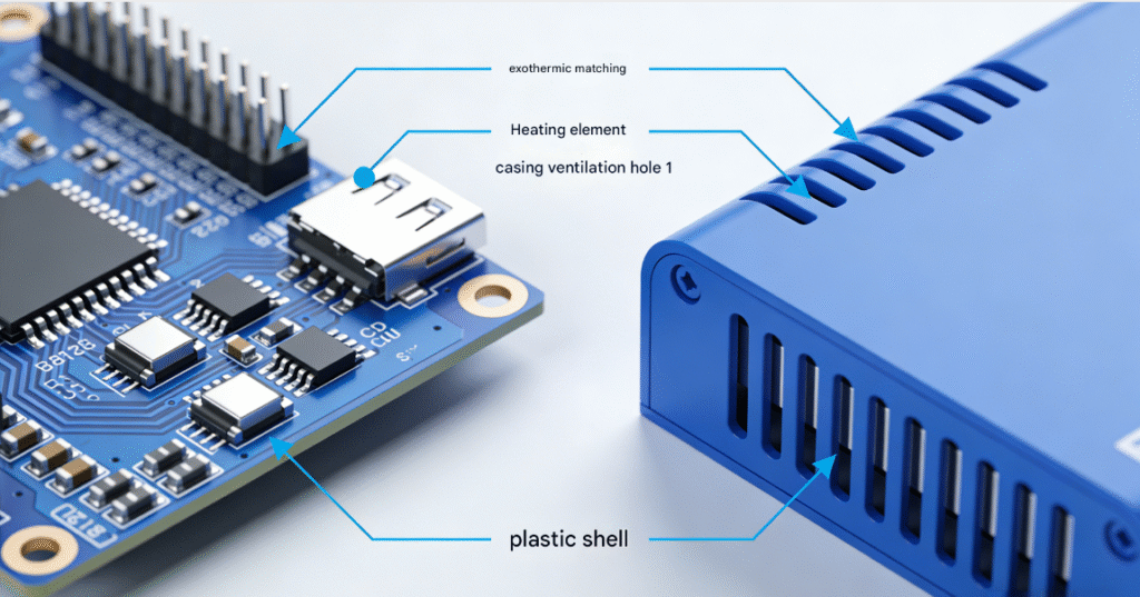
- Heat Dissipation Matching: PCB heat-generating components (e.g., power modules) should be placed directly above the vent holes of the plastic enclosure. For high-power industrial PCBs, design heat dissipation pads on the PCB that align with the enclosure’s heat sinks, ensuring efficient heat transfer. Avoid blocking enclosure vent holes with PCB components.
- EMC Compatibility: The PCB ground plane should extend to the edge of the board where possible, and the plastic enclosure should have conductive shielding layers if required by industrial EMC standards. Ensure a good electrical connection between the PCB ground and the enclosure’s grounding points to reduce electromagnetic interference.
5. Practical DFM Case Studies: Lessons from Industrial Production
Case 1: Rework Caused by Asymmetric 6-Layer Stackup
A customer in the industrial control sector commissioned a 6-layer PCB design. The initial stackup was asymmetric (Top → Signal → Power → GND → Signal → Bottom), resulting in 15% of PCBs being warped after lamination. After our team revised the stackup to a symmetric structure and adjusted the copper distribution, the warpage rate dropped to less than 3%, ensuring smooth mass production.
Case 2: Successful Mass Production with Comprehensive DFM Checks
An automotive electronics customer required a PCB that integrated SMT (Surface Mount Technology) and plastic enclosure assembly. We applied the above DFM checklist during the design phase: optimized component spacing for SMT compatibility, ensured mounting hole alignment with the enclosure, and designed heat dissipation matching. The first batch of 10,000 PCBs achieved a yield rate of 99.2%, with no assembly issues reported.
6. Conclusion: Leverage DFM to Optimize Industrial PCB Production
DFM design is a critical link between PCB design and industrial manufacturing. By strictly following the above checklist, engineers can avoid 90% of common manufacturing defects, improve production yield, and reduce costs. For industrial enterprises, partnering with a service provider that offers one-stop solutions (including PCB design, DFM pre-audit, SMT (Surface Mount Technology), plastic molding, and whole-machine assembly) can further streamline the R&D and production process.
Our team provides free DFM pre-audit services for industrial PCBs (4-layer, 6-layer, 8-layer, etc.), helping customers identify potential design issues before mass production. With years of experience in industrial electronics manufacturing, we can tailor PCB and plastic enclosure matching solutions to meet the specific needs of different industrial scenarios. Contact us today to optimize your PCB design and manufacturing process.
Pro Tip: For industrial PCBs used in harsh environments (high temperature, high humidity, vibration), additional DFM checks for mechanical strength and environmental resistance are recommended. Our one-stop service can integrate these requirements into the design phase, shortening your product R&D cycle by 30%.