If you’ve ever held a modern smartphone or opened a gaming laptop, you’ve interacted with a PCB (Printed Circuit Board)—but the “green board” you see is just the tip of the iceberg. The real magic lies in PCB layers: stacked sheets of conductive copper and insulating material that let complex circuits fit into tiny spaces without signal chaos. Unlike basic 2-layer boards (think: a simple remote), high-end devices use 16+ layers—each with a precise role. Let’s dive into exactly what these layers are, and the hyper-detailed process of building them (using a 6-layer PCB as a case study).
Part 1: PCB Layers 101—Types, Roles, and Stackups
Before we build, let’s define the “parts” of a layered PCB. Every layer falls into one of 3 categories, and their arrangement (called a stackup) dictates the board’s performance.
Common Layer Types
| Layer Type | Role | Typical Placement |
|---|---|---|
| Signal Layers | Carry electrical signals between components (e.g., data from a CPU to RAM). | Outer (top/bottom) or inner |
| Power Planes | Distribute stable voltage (e.g., 3.3V) to all components. | Inner (adjacent to ground planes) |
| Ground Planes | Act as a “reference voltage” (0V) and absorb electrical noise. | Inner (paired with power planes) |
| Dielectric Layers | Insulate copper layers to prevent short circuits. | Between all copper layers |
Example 6-Layer Stackup (High-Speed Device)
For a board handling fast signals (e.g., a Wi-Fi router), the stackup is optimized to reduce interference:
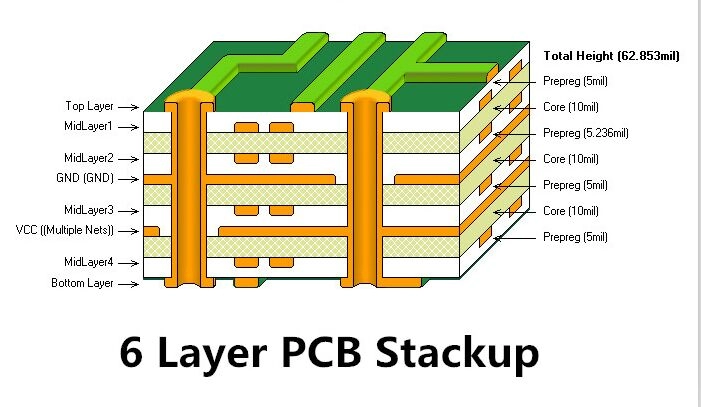
- Top Signal Layer (high-speed data)
- Ground Plane (shields top signal)
- Power Plane (3.3V)
- Inner Signal Layer (low-speed control signals)
- Ground Plane (shields inner signal)
- Bottom Signal Layer (peripheral connections)
This “signal-ground-power” pairing minimizes crosstalk (signals leaking between traces) and EMI (electromagnetic interference that could mess with other devices).
Part 2: How PCB Layers Are Produced—A Granular Walkthrough
Building a 6-layer PCB is a multi-day process that requires micron-level precision. We’ll break it into 8 stages, with details most guides skip.
Stage 1: Material Preparation (Inner Layers)
The foundation of inner layers is a core material: a sheet of dielectric (most commonly FR-4—fiberglass cloth impregnated with epoxy resin) coated on both sides with electrolytic copper foil (1oz/ft² = 35μm thick, ~half the thickness of a human hair).
- Quality check: The copper foil must have <1% surface roughness—rough spots can trap air during lamination (causing delamination later).
- Cut to size: Use a shear cutter to trim the core to the panel size (usually 18×24 inches, holding 10+ small boards).
Stage 2: Inner Layer Patterning (The “Printing” of Circuits)
This step turns the blank copper core into a functional inner signal/power layer.
Step 2.1: Clean the Copper
- Dip the core in a degreasing bath (alkaline solution) to remove oil/dust.
- Etch with a mild acid (like sulfuric acid) to “micro-etch” the copper surface—this creates tiny grooves that help the photoresist stick better.
Step 2.2: Apply Photoresist
- Use a spin coater (for small panels) or roller coater (for large batches) to apply a uniform layer of positive photoresist (light-sensitive polymer) to both sides of the core.
- Bake the board in a convection oven at 90°C for 10 minutes to dry the photoresist (too hot = brittle resist; too cold = sticky resist).
Step 2.3: Expose the Pattern
- Photomask prep: The circuit pattern is printed onto a transparent polyester film (photomask) using a high-resolution laser printer (5080 DPI—detailed enough to print 0.05mm traces).
- Alignment: Use a mask aligner to line the photomask with the core—alignment pins on the mask match holes drilled in the core (tolerance: ±0.02mm).
- UV exposure: Shine 365nm UV light on the mask/core stack for 30–60 seconds. The light polymerizes (hardens) the photoresist except where the mask’s black pattern blocks it.
Step 2.4: Develop and Etch
- Develop: Immerse the board in a developer solution (sodium carbonate) for 60 seconds. This dissolves the unhardened photoresist, revealing the copper that will become traces.
- Rinse & dry: Wash with deionized water, then blow-dry with compressed air (no lint!).
- Etch: Dip the board in a cupric chloride etching bath (45°C) for 2–3 minutes. The solution dissolves the unmasked copper—leaving only the hardened photoresist and the desired circuit pattern.
- Strip resist: Use a stripper solution (sodium hydroxide) to remove the remaining hardened photoresist, exposing the clean copper traces.
Step 2.5: Inner Layer Inspection
- AOI (Automated Optical Inspection): A camera scans the layer, comparing it to the digital circuit file (Gerber file) to detect flaws: short circuits (traces touching), open circuits (broken traces), or missing pads.
- X-ray inspection: For dense layers, X-rays check for hidden defects (e.g., copper particles trapped under resist).
- Mark defective boards: Any board with a flaw is marked with a UV ink (visible only under black light) and discarded.
Stage 3: Layer Stacking & Lamination (Bonding the Layers)
Now we combine the inner layers, dielectrics, and outer layers into a single rigid board.
Step 3.1: Prep the Stack
A 6-layer board stack (from bottom to top):
- Outer layer: FR-4 core (copper-clad)
- Prepreg: Uncured FR-4 sheet (0.1mm thick)
- Inner layer 1 (signal)
- Prepreg
- Inner layer 2 (ground)
- Core (FR-4, copper-clad)
- Inner layer 3 (power)
- Prepreg
- Inner layer 4 (signal)
- Prepreg
- Outer layer: FR-4 core (copper-clad)
- Prepreg note: Prepreg is “semi-cured” (B-stage) epoxy—when heated, it melts, flows, and cures to bond layers.
Step 3.2: Align and Laminate
- Stack alignment: Use a lamination aligner to line up all layers with alignment pins (tolerance: ±0.01mm).
- Load into press: Place the stack between stainless steel plates (to distribute pressure) and release films (to prevent sticking).
- Press cycle:
- Heat to 100°C (212°F) while applying 50 psi pressure (softens prepreg).
- Ramp heat to 175°C (347°F) over 30 minutes, increasing pressure to 300 psi (cures prepreg).
- Cool to 50°C (122°F) over 20 minutes, then release pressure.
The result: a single, rigid 6-layer board.
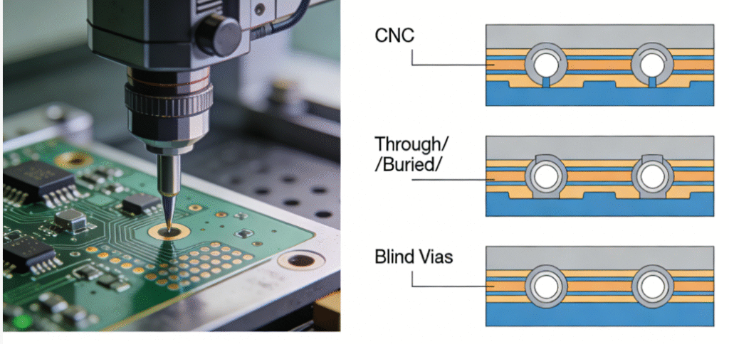
Stage 4: Drill Vias (Connecting Layers)
Vias are tiny holes that let signals/power flow between layers. There are 3 types:
- Through vias: Drill through the entire board (connects all layers).
- Blind vias: Drill from an outer layer to an inner layer (doesn’t go through).
- Buried vias: Drill between inner layers (hidden inside the board).
For our 6-layer board, we’ll drill through vias and blind vias (from top layer to inner layer 1).
Step 4.1: Drill the Holes
- CNC drilling: Use a PCB drill press with diamond-coated bits (0.1mm–1.0mm diameter). The drill spins at 100,000 RPM to prevent tearing the dielectric.
- Peck drilling: For deep holes, the bit “pecks” (drills a little, retracts to clear debris) to avoid overheating.
- Deburr: Use a brush deburrer (nylon brushes + abrasive paste) to smooth the hole edges (sharp edges can damage plating later).
Step 4.2: Via Plating (Making Holes Conductive)
- Desmear: Immerse the board in a permanganate solution to remove epoxy “smear” (leftover dielectric from drilling) from the hole walls—this ensures copper adheres.
- Palladium activation: Dip the board in a palladium chloride bath—palladium atoms stick to the hole walls, acting as a catalyst for copper plating.
- Electroless copper plating: Immerse in a copper sulfate bath (room temperature) for 30 minutes. Chemical reactions deposit a thin layer (0.5μm) of copper on the hole walls (and entire board surface).
- Electroplating: Place the board in a copper cyanide bath and apply 2A/dm² current for 60 minutes. This builds the copper layer to 25μm thick (thick enough to carry high current).
Stage 5: Outer Layer Patterning
Repeat Stage 2 (Inner Layer Patterning)—but this time on the outer copper layers (the top and bottom of the laminated board). The only difference: the outer layers include component pads (where chips/connectors will be soldered) and solder mask openings (we’ll cover this next).
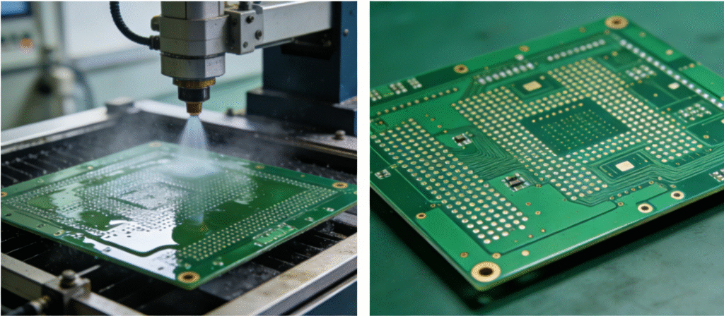
Stage 6: Solder Mask Application (The “Green” Layer)
The solder mask is a protective coating (usually green, but black/blue/red are common) that insulates copper traces, prevents short circuits, and resists moisture.
- Clean the board: Use a plasma cleaner to remove oil/dust (improves mask adhesion).
- Apply mask: Spray the board with liquid photoimageable (LPI) solder mask (a light-sensitive epoxy) and spin-coat to 25μm thickness.
- Expose mask: Use a photomask (with openings for component pads) and UV light to harden the mask except over the pads.
- Develop: Wash off the unhardened mask (revealing the pads) with sodium carbonate solution.
- Cure: Bake the board at 150°C for 60 minutes to fully cure the mask.
Stage 7: Silkscreen & Surface Finish
Step 7.1: Silkscreen Printing
- Use a screen printer to apply epoxy ink (white/black) onto the solder mask. The ink prints:
- Component designators (e.g., “R1” for resistor 1, “U2” for chip 2).
- Board outlines, logos, and “Pin 1” markers (for component alignment).
- Cure the ink at 120°C for 30 minutes.
Step 7.2: Surface Finish (Protecting Pads)
Copper pads oxidize quickly (which ruins solderability), so we apply a protective finish:
- HASL (Hot Air Solder Leveling): Dip the board in molten solder (63% tin, 37% lead) then blow hot air to smooth the solder—creates a thick, durable finish (cheap, but not for fine-pitch components).
- ENIG (Electroless Nickel Immersion Gold): Plate pads with 5μm nickel, then 0.05μm gold—flat, corrosion-resistant, ideal for smartphones/laptops.
- OSP (Organic Solderability Preservative): Apply a thin organic film (0.1μm) to pads—low-cost, eco-friendly, but less durable than ENIG.
Stage 8: Final Testing & Singulation
Step 8.1: Electrical Testing
- Flying Probe Test: A machine with 4–8 “probes” touches every pad/via, checking:
- Continuity: Does current flow between connected traces?
- Isolation: Do unconnected traces have infinite resistance (no shorts)?
- Bed of Nails Test: For high-volume production, a custom fixture with hundreds of pins tests the board in 1–2 seconds.
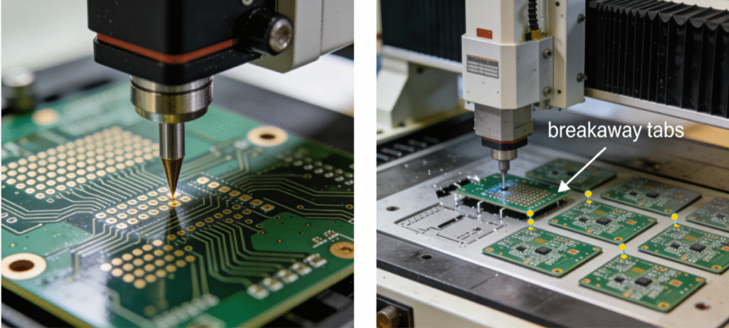
Step 8.2: Singulation (Cutting into Individual Boards)
- The laminated panel has 10+ small boards—use a routing machine (CNC router with a diamond bit) to cut along the “breakaway tabs” (small connections between boards).
- Alternatively, use a laser cutter (for fine-pitch boards) to cut without mechanical stress.
Step 8.3: Final Inspection
- Check for:
- Solder mask bubbles, misaligned silkscreen, or damaged pads.
- Correct surface finish thickness (measured with a micrometer).
- Package the boards in anti-static bags (to protect against ESD) for shipping.
Part 3: Why This Matters (Beyond “Green Boards”)
Every step in this process is critical:
- A 0.01mm alignment error = a via that misses a trace.
- A dirty photoresist = a short circuit.
- A poorly cured prepreg = delamination (layers peeling apart) when the board gets hot.
This precision determines the difference in manufacturing complexity for PCBs with different numbers of layers—but it is precisely these meticulous processes that enable modern electronic devices to achieve their compact, high-speed, and reliable characteristics.