1. Introduction
In the field of electronic R&D, there is a prevalent pain point: a 6-layer PCB prototype that performs flawlessly in the lab often hits a wall during mass production—either the yield rate drops below 50%, or fatal defects like warping and short circuits occur, ultimately leading to extended R&D cycles and doubled costs. The core cause behind this is often the neglect of manufacturing constraints during the design phase.
In our previous article, we broke down the complete manufacturing process of 6-layer PCBs, covering everything from inner layer patterning and lamination to drilling, solder mask application, and final singulation. Each step comes with clear process constraints. This article will focus on the design side, sharing a set of DFM (Design for Manufacturability) rules tailored to actual manufacturing needs. We will cover key aspects such as stackup design, via layout, and line width/space specifications, helping you avoid manufacturing risks from the source and ensure your design smoothly transitions to mass production.
2. Core Design Principle: Align Designs with Manufacturing Capabilities
For 6-layer PCB design, DFM (Design for Manufacturability) is not an option but a core principle that must be followed throughout the process. Simply put, the essence of DFM is “thinking from the manufacturer’s perspective”—when designing, you need to meet not only the circuit performance requirements but also fully consider the factory’s processing capabilities, avoiding the situation where a design is theoretically feasible but impossible to manufacture.
Before starting the design, it is recommended to confirm three core manufacturing constraints with your PCB supplier to avoid rework later:
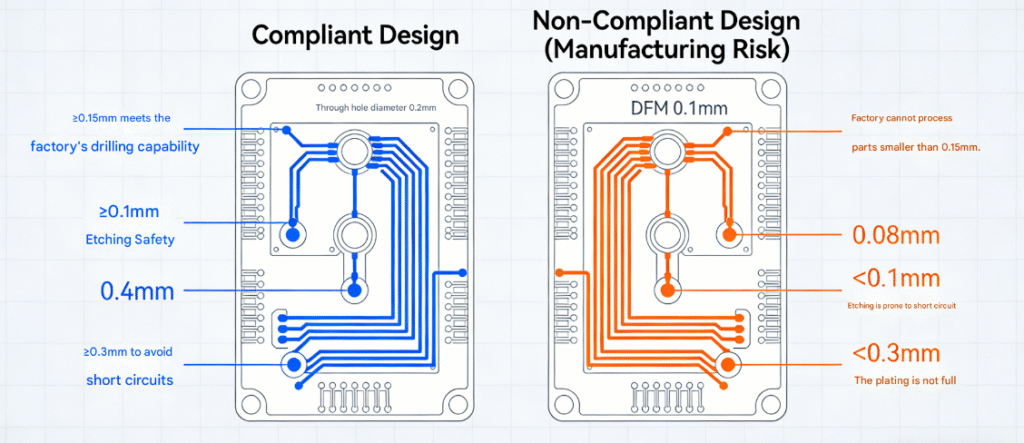
- Minimum CNC drilling aperture limit: Standard mass-production factories typically have a minimum drilling capability of ≥0.15mm. If your design requires smaller apertures (such as 0.1mm micro-vias), you must confirm in advance whether the supplier has high-precision drilling equipment, noting that micro-vias will increase manufacturing costs.
- Lamination temperature and pressure tolerance: 6-layer PCB lamination is typically completed under high temperature (175°C) and high pressure (300psi). When designing the stackup, ensure uniform thickness across all layers to prevent warping caused by uneven prepreg distribution after lamination.
- Etching precision: The etching precision in mass production is usually ±0.02mm. Therefore, the minimum recommended design value for line width/space is ≥0.1mm (for 1oz copper thickness). If your design includes line width/space smaller than 0.08mm, confirm whether the supplier has high-precision etching technology.
3. Critical Design Step 1: Optimize Stackup Design for Both Performance and Manufacturability
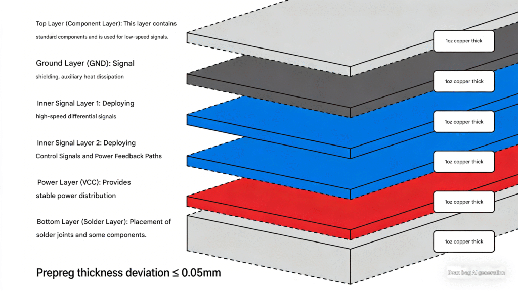
The stackup design of a 6-layer PCB directly impacts two core aspects: electromagnetic interference (EMI) control and lamination difficulty. An unreasonable stackup not only causes signal interference and performance degradation but may also lead to lamination defects due to uneven thickness. Below is a universal industrial-grade 6-layer stackup solution (top to bottom) that has been validated in numerous mass production projects, suitable for most mid-to-high-end applications such as industrial control and automotive electronics:
- Top Layer (Component Layer): Prioritize low-speed signals and common components. Avoid densely routing high-speed signals on the top layer to reduce signal interference.
- Ground Layer: As a complete ground plane, it not only provides shielding for the top-layer signals but also aids heat dissipation. It is recommended to cover at least 80% of the layer area.
- Inner Signal Layer 1: Dedicated to high-speed signals (e.g., USB 3.0, Ethernet, CAN bus). With the shielding effect of the upper and lower ground planes, signal crosstalk is minimized.
- Inner Signal Layer 2: Can be used for secondary signals or as a power layer (e.g., supplying 3.3V to core chips). Ensure a reasonable spacing from adjacent signal layers.
- Power Layer: Provides stable voltage for the entire circuit. A complete plane design is recommended to reduce power supply noise.
- Bottom Layer (Solder Layer): Can accommodate auxiliary components and secondary signals, complementing the top layer to balance the weight distribution of the PCB and reduce the risk of lamination warping.
In stackup design, focus on avoiding two common mistakes:
- Placing two high-speed signal layers adjacent to each other without a ground plane for isolation—this design causes severe signal crosstalk, not only affecting circuit performance but also increasing debugging difficulty due to signal integrity issues.
- Uneven prepreg thickness distribution—for example, some areas have overly thick prepreg while others are too thin. This leads to PCB warping due to uneven stress during lamination. It is recommended to ensure the thickness deviation of prepreg between layers does not exceed 0.05mm.
4. Critical Design Step 2: Via Layout and Specifications to Avoid Drilling and Plating Issues
Vias are the core structures that enable interlayer connections in 6-layer PCBs. There are three common types: through vias, blind vias, and buried vias (refer to our previous manufacturing process article for specific differences). Different via types vary significantly in manufacturing difficulty and cost. Designers should select the appropriate type based on actual needs and follow these DFM rules:
1. Via Type Selection Recommendations
- Through Vias: Lowest manufacturing cost and most mature technology, suitable for most interlayer connection scenarios. The disadvantage is that they occupy space on both the top and bottom layers, making them unsuitable for high-density designs.
- Blind/Buried Vias: Blind vias only connect surface layers to inner layers, while buried vias only connect inner layers to each other. Both save surface space and are suitable for high-density designs, but they require more complex manufacturing processes, increasing costs by 20%-30%. It is recommended to use them only in high-density scenarios (e.g., smartphone motherboards, precision sensors).
2. Via Specification and Layout Rules
- Via Diameter and Pad Matching: For conventional through vias, it is recommended to design with aperture ≥0.15mm and pad diameter ≥0.3mm. This specification perfectly matches the drilling and plating processes of standard factories, avoiding drilling deviation caused by overly small apertures or insufficient plating due to undersized pads.
- Spacing Between Adjacent Vias: The center-to-center spacing between any two vias should be ≥0.3mm. If the spacing is too small, metal ions cannot uniformly cover the via walls during plating, leading to cold solder joints or short circuits.
- Via Placement Taboos: Never place vias on component pads, as this causes solder to flow into the vias during soldering, resulting in cold joints. Additionally, avoid placing vias within 5mm of the PCB edge to prevent via cracking during singulation.
Common Mistake Reminder: Many engineers pursue compact designs by directly specifying micro-vias smaller than 0.1mm without confirming the factory’s capabilities, or overusing blind/buried vias in low-density PCBs. The former may make the design unmanufacturable, while the latter leads to unnecessary cost waste. It is recommended to fully communicate with the supplier before finalizing the design.
5. Critical Design Step 3: Line Width, Line Space, and Pad Design—Details Determine Yield
Line width, line space, and pad size are the most basic details in PCB design, yet they are the most frequent causes of manufacturing defects. Especially for 6-layer PCBs with multiple inner signal layers, inner layer etching is more challenging, requiring extra caution during design. Below are standard specification recommendations suitable for mass production (adjustable based on copper thickness and factory grade):
1. Line Width and Line Space
For 6-layer PCBs with 1oz copper thickness (approximately 0.35mm), we recommend:
- For regular signals (e.g., GPIO): Line width ≥0.1mm, line space ≥0.1mm.
- For power lines (e.g., 5V, 12V power supply): Adjust the width based on current requirements. It is recommended to increase the line width by 0.3mm for every additional 1A of current (e.g., a 2A power line should have a width ≥0.6mm) to avoid overheating due to insufficient line width.
- For high-frequency signals (e.g., above 1GHz): Line width should be designed to meet impedance control requirements (e.g., a 50Ω impedance microstrip line has a width of approximately 0.8mm). At the same time, ensure the line space is ≥3 times the line width to reduce crosstalk.
2. Pad Size
Pad size directly affects soldering quality. Here are design recommendations for different component types:
- For SMD components (0402 size): Pad length ≥0.8mm, width ≥0.4mm, spacing between two pads ≥0.3mm.
- For SMD components (0603 size): Pad length ≥1.0mm, width ≥0.5mm, spacing ≥0.4mm.
- For through-hole components (e.g., through-hole resistors, connectors): Pad diameter ≥1.5 times the aperture (e.g., a through-hole with a 0.2mm aperture requires a pad diameter ≥0.3mm) to ensure sufficient solder wraps around the pins during soldering.
Common Mistakes to Avoid: Designing line width/space smaller than 0.08mm for non-high-precision factories, leading to short circuits or open circuits during etching; or designing overly small pads to save space, resulting in component detachment or cold solder joints after soldering.
6. Additional DFM Tips to Improve Manufacturing Yield
In addition to the core design steps above, the following details can effectively improve the manufacturing yield of 6-layer PCBs:
- Board Edge Design: The distance between components and the PCB edge should be ≥5mm. At the same time, reserve a 3–5mm “process edge” on the board edge (for factory positioning and processing) to prevent component damage by cutting tools during singulation.
- Copper Balance: If there are large blank areas on the PCB (no traces or pads), add “dummy copper” (copper foil without electrical connections) to ensure uniform copper coverage across the PCB (with a coverage difference of no more than 20%). This prevents warping caused by uneven stress during etching and lamination.
- Silkscreen Design: Silkscreens are used to mark component models and positions. Avoid printing silkscreens on pads—this blocks solder paste and causes poor soldering. Additionally, the recommended size for silkscreen characters is ≥1.2mm×0.6mm to ensure clarity and readability.
- Pre-Delivery Self-Inspection: Before sending design files (Gerber files) to the factory, complete a 5-item self-inspection: ① Are line width/space compliant with factory requirements? ② Are via specifications and layout reasonable? ③ Is the stackup structure clear? ④ Are pad sizes matched to components? ⑤ Are there any redundant floating traces or isolated copper foils?
7. Conclusion
The core of 6-layer PCB design is to balance performance requirements and manufacturability. More often than not, a more precise design is not necessarily better—one that aligns with actual manufacturing capabilities is more likely to ensure mass production yield and control costs. The DFM rules shared in this article are summarized from extensive mass production practices. Optimizing details in every step, from stackup and via design to line width and pad specifications, can eliminate manufacturing issues at the source.
Pro Tip: As the core control unit of industrial products, 6-layer PCBs require high compatibility between their shape design, mounting methods and plastic enclosures. While providing PCB manufacturing, SMT and testing services, we also offer plastic mold development, plastic part injection molding and complete product assembly. From PCB design optimization to plastic structure adaptation, and final product assembly & testing, we deliver one-stop solutions that cut your product R&D cycle by 30%.
If you have encountered problems such as warping, short circuits, or low yield rates during 6-layer PCB design or manufacturing, feel free to share your experiences in the comments section. Follow us for more PCB technical insights. In our next article, we will focus on “PCB Material Selection Guide for 6-Layer Industrial-Grade Circuit Boards” to help you further improve product reliability.